Mastering power integrity PCB measurement is essential for high-speed digital design. This guide explains how to use a VNA for PDN impedance analysis, ensuring reliable power delivery in your high-speed PCB projects. We cover setup, calibration, and interpretation of results.
Why VNA is the Preferred Tool for Power Integrity PCB Measurement
In modern high-speed systems, power integrity (PI) is as critical as signal integrity. The Power Distribution Network (PDN) must deliver stable, low-noise voltage to active devices. Any impedance peak can cause voltage ripple, jitter, and functional failure. The most reliable method to characterize PDN performance is measuring its impedance profile across frequency using a Vector Network Analyzer (VNA).
What is PDN Impedance?
The PDN impedance (Z_PDN) is the frequency-dependent resistance and reactance seen from the power/ground terminals of a device. Ideally, it should be flat and low across the entire frequency range of interest (typically DC to several GHz). In reality, the impedance profile exhibits peaks due to resonances between decoupling capacitors, PCB plane capacitance, and parasitic inductances.
Advantages of VNA for PDN Measurement
While impedance analyzers and oscilloscopes can be used, the VNA offers distinct advantages for high-frequency PDN characterization:
- Broad Frequency Range: VNAs can sweep from low kHz to tens of GHz, capturing both low-frequency bulk capacitor behavior and high-frequency plane resonances.
- High Dynamic Range: They measure small impedance variations accurately, even in the milliohm range.
- Phase Information: The VNA provides both magnitude and phase, enabling complex impedance analysis (real vs. imaginary parts).
- S-Parameter to Impedance Conversion: By measuring S11 (reflection coefficient), the VNA can directly compute input impedance at the measurement port.
Key Parameters: S11, Z11, and the PDN Profile
The fundamental measurement is the reflection coefficient (S11) at the power rail. From S11, the impedance Z11 is calculated using the formula: Z11 = Z0 * (1 + S11) / (1 – S11). Where Z0 is the system reference impedance (typically 50 ohms). The resulting Z11 profile shows impedance vs. frequency, revealing resonance peaks and overall PDN health.
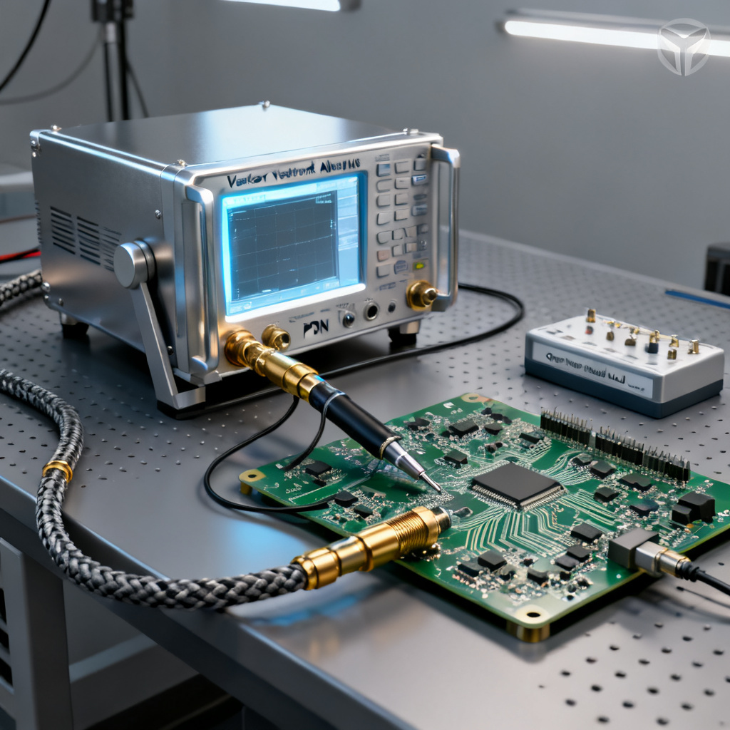
Equipment and Setup for Power Integrity PCB Measurement
Essential Equipment List
- Vector Network Analyzer: A 2-port VNA covering at least DC to 6 GHz (for most high-speed digital PCBs). Ensure it supports low-frequency operation (e.g., starting at 10 kHz or lower).
- Calibration Kit: A precision open, short, load (OSL) kit rated for the frequency range. For PDN work, a SOLT (Short-Open-Load-Through) calibration is standard.
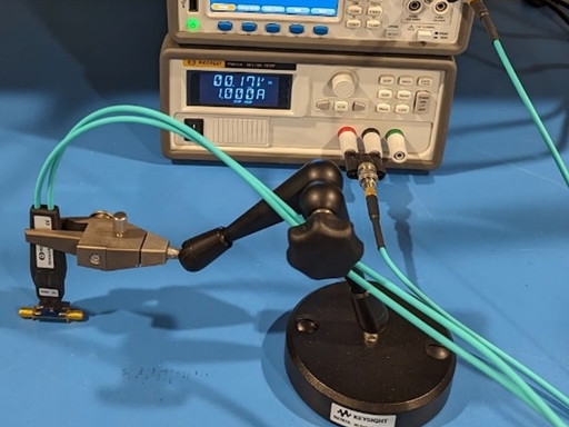
- Probes and Cables: Low-loss, phase-stable coaxial cables. For PDN probing, use a dedicated PDN probe (e.g., from Picotest or Keysight) or a homemade probe with a 50-ohm termination and a DC block.
- Power Supply: The device under test (DUT) must be powered during measurement.
- Software: VNA control software (e.g., Keysight VNA software, open-source scikit-rf) for data analysis.
Choosing the Right Probe for Power Integrity PCB Measurement
Power integrity PCB design : For PDN impedance measurement, the probe must have low parasitic inductance, DC blocking capability, and 50-ohm impedance. Use a probe with a ground spring or a coaxial probe tip. Recommended probe types include the Picotest PDN Probe (specifically designed for PI measurements) or a homemade probe using a 50-ohm semi-rigid cable with a short pin and ground ring (tip length < 1 mm).
DUT Preparation
- Power the Board: The PDN must be powered at its nominal voltage. The VNA measures the impedance of the powered PDN, which includes the dynamic behavior of regulators and capacitors.
- Access Points: Identify a via or test point on the power rail and ground. Solder a small coaxial connector (e.g., SMA or U.FL) or use a probe landing pad.
- Decoupling Capacitors: Keep all decoupling capacitors in place. The measurement should reflect the actual operating condition.
Calibration for Accurate Power Integrity PCB Measurement
Why Calibration is Essential
Without calibration, the measurement includes the effects of cables, connectors, and the probe. Calibration mathematically removes these errors, leaving only the DUT’s impedance.
Calibration Types for PDN Measurement
- SOLT (Short-Open-Load-Through) Calibration: The standard for 1-port (S11) measurements. Perform at the probe tip.
- OSL (Open-Short-Load) Calibration: Sufficient if measuring only reflection. The “Load” must be a precision 50-ohm standard.
Step-by-Step Calibration Procedure
- Set Up the VNA: Define the frequency sweep (e.g., 10 kHz to 10 GHz), number of points (e.g., 1601), and IF bandwidth (e.g., 1 kHz).
- Connect the Calibration Kit: Attach the open, short, and load standards to the end of the test cable or probe.
- Perform Calibration: Use the VNA’s calibration wizard. For a 1-port measurement, select “Reflection” and follow prompts for open, short, and load.
- Verify Calibration: Measure a known load (e.g., a 50-ohm resistor). The displayed S11 should be < -40 dB across the frequency range.
- Save Calibration: Store the calibration file for future use.
Important: For PDN measurements, the calibration must be done at the probe tip, not at the VNA port. This ensures that the probe’s own impedance is de-embedded.
De-Embedding the Probe
If your probe has significant parasitic inductance (e.g., > 1 nH), consider de-embedding. Use the VNA’s port extension or a 2-tier calibration: first tier calibrates at the VNA port; second tier measures the probe’s S-parameters using a known standard (e.g., a short circuit) and mathematically subtracts them.
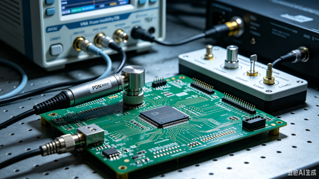
Measurement Procedure for Power Integrity PCB Measurement
Connect the DUT
- Attach the calibrated probe to the power rail via the test point.
- Ensure the ground connection is as short as possible (use a ground spring or adjacent via).
- Verify the board is powered and stable.
Set VNA Parameters
| Parameter | Recommended Setting for Power Integrity PCB Measurement |
|---|---|
| Start Frequency | 10 kHz or lower (to capture bulk capacitor behavior) |
| Stop Frequency | At least 10x the highest frequency of interest (e.g., 10 GHz for 1 Gbps signals) |
| Number of Points | 1601 points for high resolution |
| IF Bandwidth | 1 kHz (lower = better noise performance, but slower sweep) |
| Averaging | Enable averaging (e.g., 10 averages) to reduce noise |
Take the Measurement
- Run the sweep. The VNA will display S11 (log magnitude and phase) or Z11 (converted).
- Save the data as a .s1p file (Touchstone format).
Convert S11 to Impedance
Most VNAs can directly plot Z11 (in ohms) vs. frequency. If not, use the formula: Z = 50 * (1 + S11) / (1 – S11). Plot the result on a log-log scale (impedance vs. frequency).
Repeat for Multiple Locations
For a comprehensive PDN analysis, measure at multiple power rail points (e.g., near the VRM, near the load, at board edges). This helps identify local resonances.
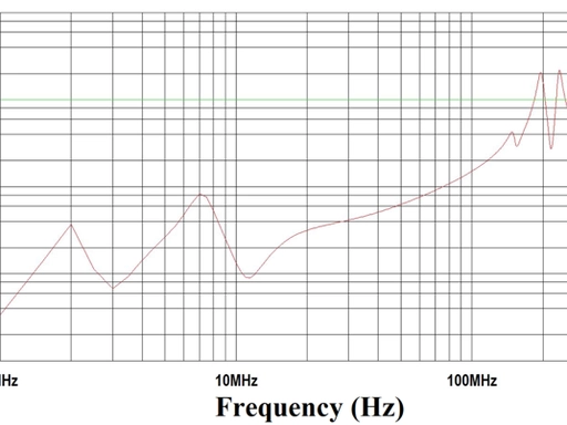
Interpreting the PDN Impedance Profile
The Ideal Profile
A healthy PDN should have impedance below the target impedance (Z_target) across all frequencies. Z_target is calculated as: Z_target = (V_rail * Ripple_allowable) / I_transient. For example, a 1.8V rail with 5% ripple (90 mV) and a 1A transient requires Z_target < 90 mΩ.
Common Features in the Profile
- Low-Frequency Region (DC to ~1 MHz): Dominated by the VRM output impedance and bulk capacitors. Impedance should be low (milliohms).
- Mid-Frequency Region (1 MHz to 100 MHz): Controlled by ceramic decoupling capacitors. Expect impedance dips and peaks due to capacitor self-resonance.
- High-Frequency Region (>100 MHz): Governed by PCB plane capacitance and package parasitics. Impedance peaks indicate plane resonances.
Identifying Resonance Peaks
Resonance peaks are the biggest threat to power integrity. They occur when inductive and capacitive reactances cancel, creating high impedance. Key indicators: sharp peaks indicate high Q-factor resonances; broad peaks may indicate multiple overlapping resonances; compare the frequency of peaks to the operating frequency of the device.
Using the Phase Plot
The phase of Z11 reveals whether the impedance is inductive (positive phase) or capacitive (negative phase). At resonance, the phase crosses zero. This helps in identifying the nature of the impedance.
Troubleshooting and Optimization Based on VNA Results
Reducing Low-Frequency Impedance
- Add more bulk capacitors near the VRM.
- Improve VRM bandwidth using a faster regulator or add a feed-forward capacitor.
Damping Mid-Frequency Resonances
- Add a damping capacitor with higher ESR (e.g., tantalum) to reduce Q.
- Use a ferrite bead in series with the power rail to add loss.
Suppressing High-Frequency Plane Resonances
- Add decoupling capacitors near the load using multiple values (e.g., 100 pF, 1 nF, 10 nF) to cover a broad frequency range.
- Reduce plane spacing (thinner dielectric between power and ground planes increases plane capacitance).
- Use a power plane with a cutout to isolate noisy sections.
Verifying Changes
After making modifications, re-measure the PDN impedance. The goal is to lower all peaks below Z_target. Iterate until the profile is smooth and low.
Advanced Considerations for High-Speed PCBs
Measuring Under Dynamic Load
The VNA measures small-signal impedance. For large-signal transient behavior, combine VNA results with time-domain measurements (e.g., using an oscilloscope with a current probe).
Multi-Port PDN Measurements
For complex boards with multiple power rails, use a 4-port VNA with a switching matrix to measure cross-impedance (Z12, Z21). This reveals coupling between rails.
Simulation Correlation
Compare VNA measurements with simulation results (e.g., from Ansys SIwave or Cadence Sigrity). Discrepancies indicate model inaccuracies (e.g., missing parasitic inductance).
Handling Very Low Impedance (< 1 mOhm)
At very low impedances, the VNA’s noise floor becomes limiting. Use a low-IF bandwidth (100 Hz) and high averaging. Consider using a differential probe with a balun.
Common Mistakes and How to Avoid Them
| Mistake | Consequence | Solution |
|---|---|---|
| Not powering the DUT | Measures passive PDN only, missing VRM effects | Always power the board during measurement |
| Using a long probe tip (> 2 mm) | Adds inductance, causing false high-frequency peaks | Keep probe tip < 1 mm, use ground spring |
| Poor calibration | Incorrect impedance values | Calibrate at probe tip, verify with known load |
| Ground loop interference | Noise on measurement | Use isolated power supply, single-point ground |
| Ignoring DC block | Damages VNA | Always use DC block or probe with built-in blocking |
Frequently Asked Questions about Power Integrity PCB Measurement
What is the main purpose of using a VNA for power integrity PCB measurement?
The main purpose is to measure the PDN impedance profile across frequency, identifying resonance peaks that can cause voltage ripple and signal integrity issues in high-speed designs. This power integrity PCB measurement ensures the PDN meets target impedance requirements.
How do I calibrate a VNA for PDN impedance measurement?
Perform an OSL or SOLT calibration at the probe tip. Use precision open, short, and load standards. Verify with a known 50-ohm load. This step is critical for accurate power integrity PCB measurement.
What is the target impedance for a typical PDN?
The target impedance is calculated as Z_target = (V_rail * Ripple_allowable) / I_transient. For a 1.8V rail with 5% ripple and 1A transient, Z_target is 90 mΩ. This value guides your power integrity PCB measurement goals.
Can I use a VNA without powering the board?
No. The PDN must be powered to capture the dynamic behavior of VRMs and decoupling capacitors. Unpowered measurements miss critical effects, compromising your power integrity PCB measurement accuracy.
What probe is best for VNA-based PDN measurement?
A dedicated PDN probe (e.g., Picotest) with low inductance and built-in DC blocking is ideal. Alternatively, a homemade probe with a 50-ohm semi-rigid cable and short ground tip works. The probe directly impacts your power integrity PCB measurement quality.
Why Choose Our High-Speed PCB Manufacturing for Power Integrity
We specialize in high-speed PCB fabrication with integrated power integrity PCB measurement services. Our in-house VNA testing validates PDN impedance profiles, ensuring your designs meet stringent performance targets. Unlike generic PCB manufacturers, we provide detailed impedance reports and optimization recommendations for each prototype run. Our expertise in high-speed materials and controlled impedance stackups directly supports accurate power integrity PCB measurement from design to production.
Glossary of Key Terms in Power Integrity PCB Measurement
- PDN: Power Distribution Network – the network delivering power from the regulator to the load.
- VNA: Vector Network Analyzer – an instrument measuring S-parameters to characterize impedance.
- S11: Reflection coefficient – indicates how much signal is reflected from the port.
- Z11: Input impedance at the measurement port, derived from S11.
- Target Impedance (Z_target): The maximum allowable PDN impedance to ensure stable voltage.
- Resonance Peak: A frequency where PDN impedance spikes due to LC resonance.
- De-embedding: Mathematical removal of probe and cable effects from measurement data.
- SOLT Calibration: Short-Open-Load-Through calibration standard for VNA accuracy.