Mastering Reflection in Transmission Line Simulation in Keysight ADS is essential for high-speed PCB design. Signal reflections caused by impedance discontinuities are the primary source of data corruption, jitter, and electromagnetic interference (EMI). For B2B manufacturers, understanding and simulating these reflections is critical for first-pass success. This comprehensive guide provides a step-by-step methodology to model, simulate, and analyze transmission line reflections using Keysight Advanced Design System (ADS).

Why Reflection in Transmission Line Simulation in Keysight ADS Matters for High-Speed PCB
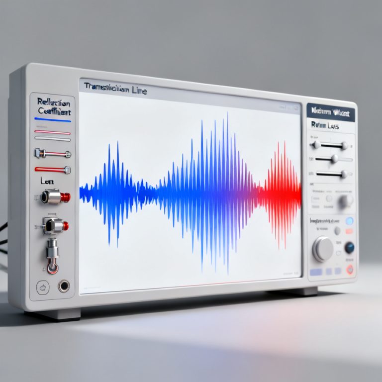
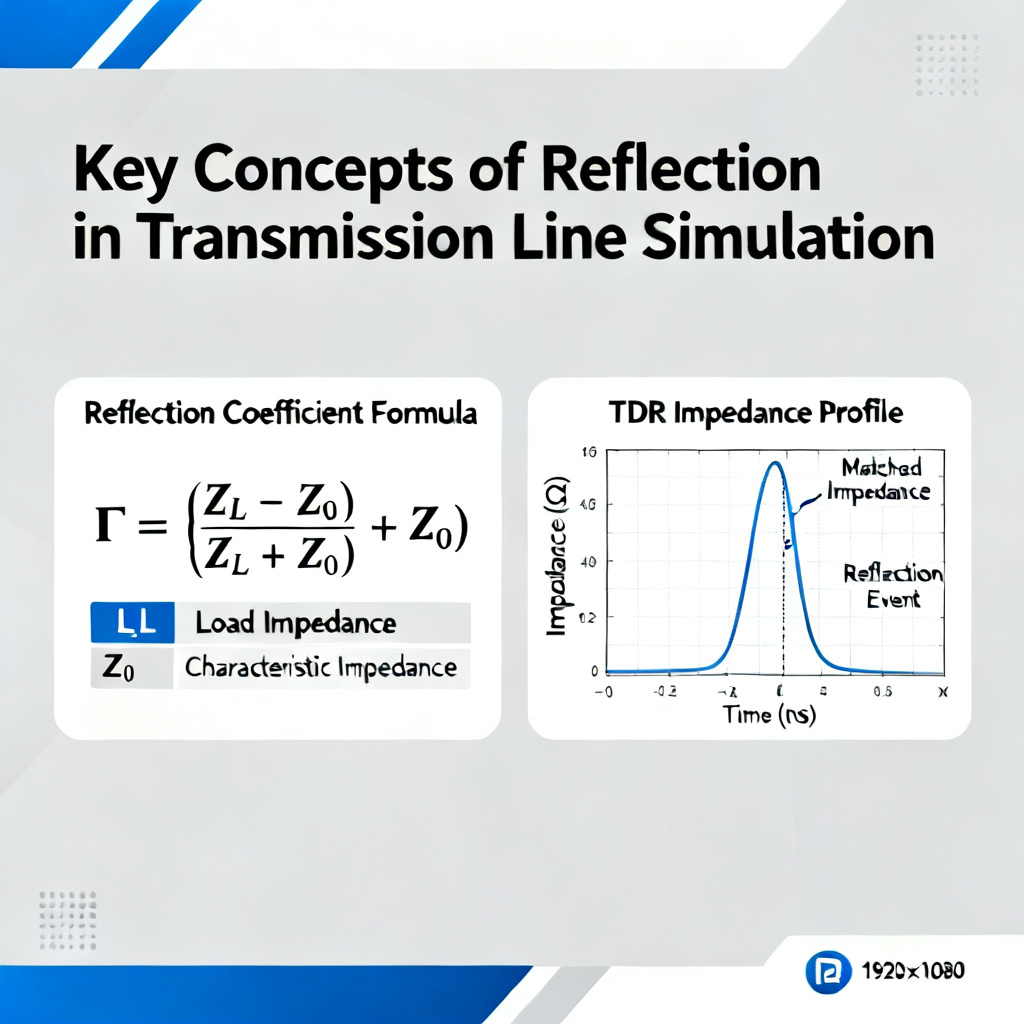
Reflection in Transmission Line Simulation in Keysight ADS begins with understanding the physics. A reflection occurs when a signal encounters an impedance mismatch such as a change in trace width, a via, or a connector. The reflection coefficient (Γ) is defined as: Γ = (Z_load – Z_0) / (Z_load + Z_0). A perfect match (Γ = 0) means zero reflection. Any mismatch (Γ ≠ 0) causes part of the signal energy to bounce back, distorting the waveform. In high-speed PCBs operating at 10 Gbps or higher, even a 5% impedance mismatch can cause significant eye closure.
Step 1: Setting Up Your Workspace for Reflection in Transmission Line Simulation in Keysight ADS
1.1 Create a New Project and Schematic
Open ADS and navigate to File > New > Project. Name it appropriately (e.g., Reflection_TL_Simulation). Create a new schematic: Schematic > New Schematic (e.g., TL_Reflection_Test).
1.2 Choose the Correct Simulation Environment
For Reflection in Transmission Line Simulation in Keysight ADS, use Transient (Time-Domain) Simulation for digital signals like pulses and PRBS, employing the Envelope or Transient controller. Use S-Parameter (Frequency-Domain) Simulation for impedance profiling via TDR-like analysis and reflection coefficient (Γ) plots, employing the S-Parameter controller. For a complete reflection study, run both simulations: time-domain shows waveform distortion, while frequency-domain reveals the exact impedance profile.
Step 2: Modeling the Transmission Line with Discontinuities for Reflection Analysis
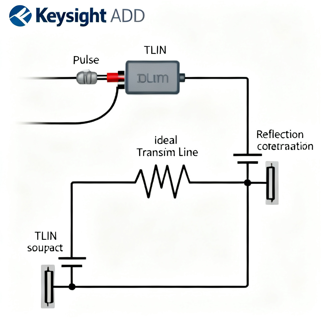
2.1 Using Ideal Transmission Line Models
From the TLines-Ideal palette, drag TLIN (Ideal Transmission Line) and set Z0 (e.g., 50Ω) and EL (electrical length, e.g., 90° at 1 GHz). Use TLOC (Open Stub) or TLSC (Short Stub) to simulate a mismatch. Connect a 50Ω source to a TLIN with Z0=50Ω, then add a TLIN with Z0=75Ω in series to simulate a sudden impedance bump, creating a reflection.
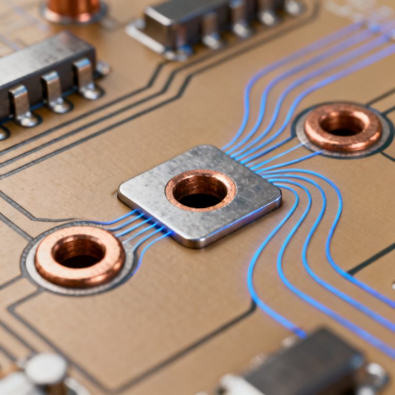
2.2 Modeling Real-World Discontinuities for PCB-Specific Reflection
For accurate B2B PCB simulation, use Via Models (ML_VIA from the TLines-Microstrip palette) with via diameter, pad size, and anti-pad settings, as a via creates a capacitive discontinuity. Use MBEND (Microstrip Bend) for bends, where a 90° bend adds excess capacitance (~0.01 pF) and mitered bends reduce reflection. Use S-Parameter file blocks (SnP) for connectors like SMA or USB-C, which are often the largest reflection sources.
2.3 Importing Stackup Data for Physical Models
For a real PCB such as 4-layer FR4, use the Layer Setup in ADS to define dielectric constant (Er = 4.2 for FR4), copper thickness (1 oz = 35 µm), and substrate height (e.g., 0.2 mm for microstrip). Then use TLines-Microstrip components like MLIN (Microstrip Line) to calculate Z0 and propagation delay based on the stackup.
Step 3: Simulating Reflection Using Time-Domain (Transient) in Keysight ADS
3.1 Configure the Transient Controller
Place a TRANSIENT controller from the Simulation-Transient palette. Set StopTime to 10 ns (enough for 2-3 round trips) and MaxTimeStep to 1 ps (to capture fast edges).
3.2 Set Up the Source Stimulus
Use a Pulse source from Sources-Time Domain. Set Vlow = 0V, Vhigh = 1V, Rise = 50 ps (typical for 10 Gbps signals), Width = 500 ps, and Period = 1 ns. Add a Term (50Ω) at the source to avoid source reflection.
3.3 Add Measurement Probes
Place Vout pins at the source, at the discontinuity, and at the load. Use Vt (voltage vs. time) in the data display.
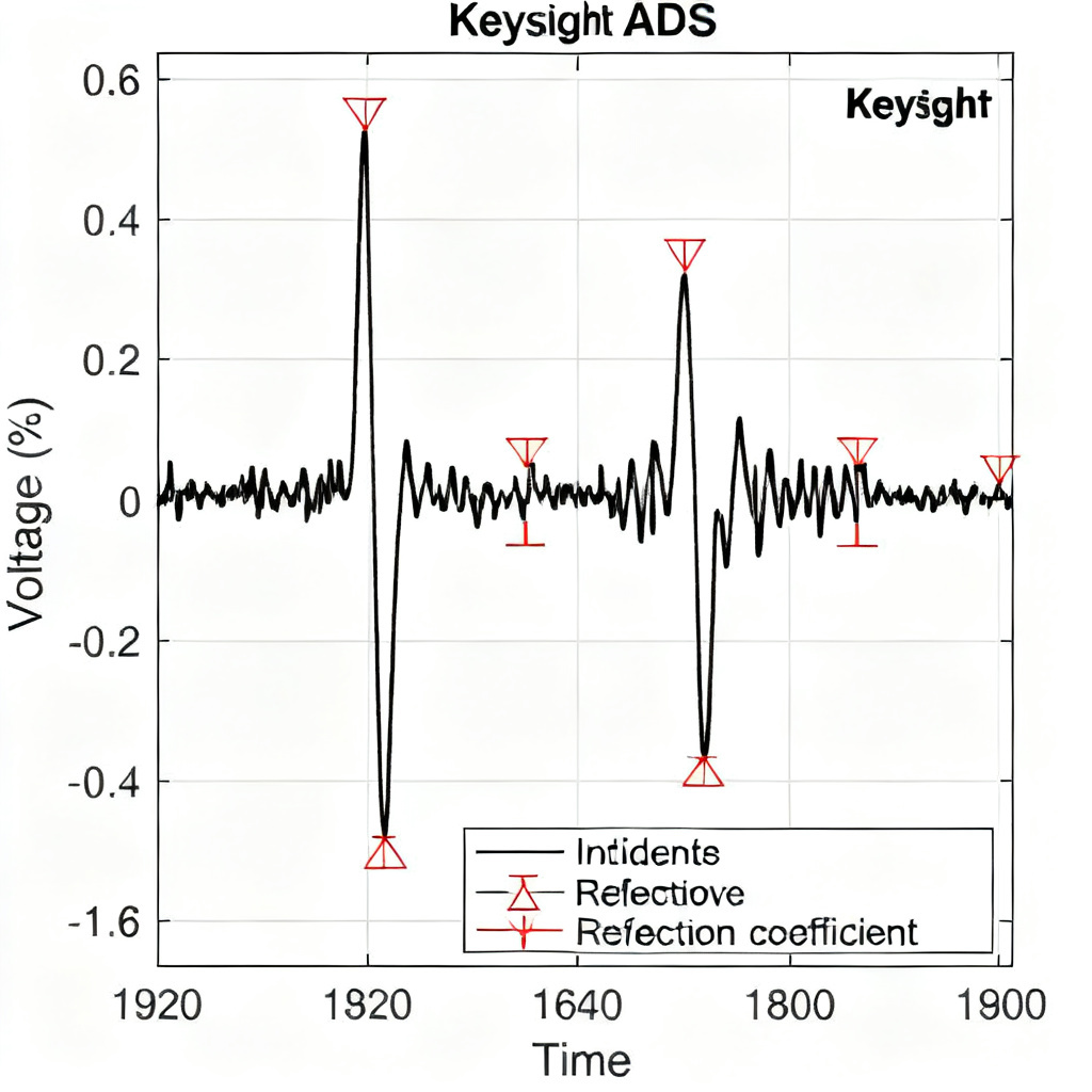
3.4 Analyze the Reflection Waveform
Run the simulation. The plot shows the Incident Wave (the initial pulse, e.g., 1V) and the Reflected Wave (a smaller pulse returning after 2*Td round-trip delay). For a 75Ω bump (Z_load > Z0), the reflected pulse is positive (same polarity). For a 30Ω bump (Z_load < Z0), it is negative (opposite polarity). At the source, the incident and reflected waves add, causing overshoot or undershoot. The Reflection Coefficient (Γ) can be visually estimated as Γ = V_reflected / V_incident.
Step 4: Simulating Reflection Using Frequency-Domain (S-Parameters & TDR)
4.1 Set Up S-Parameter Simulation
Place an S-Parameter controller. Set Frequency range from 10 MHz to 20 GHz (for high-speed signals) and NumPoints to 1001.
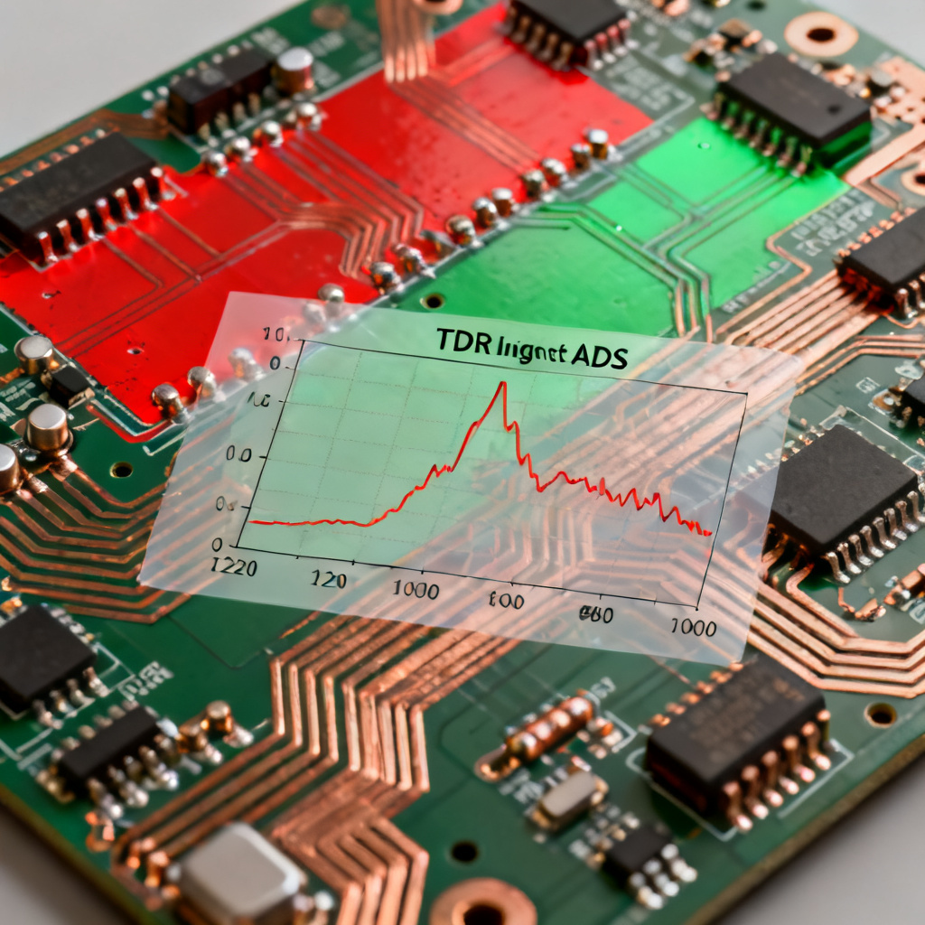
4.2 Use TDR (Time Domain Reflectometry) for Impedance Profile
ADS has a built-in TDR function. After S-parameter simulation, in the data display, write: TDR = tdr(S11, 50, time). This calculates the impedance vs. time (or distance) profile from the reflection data (S11). A flat line at 50Ω means perfect match. A spike up (e.g., 75Ω) indicates an inductive or high-impedance discontinuity. A dip down (e.g., 30Ω) indicates a capacitive or low-impedance discontinuity.
4.3 Measure S11 (Return Loss)
Plot dB(S(1,1)) vs. frequency. A lower value (e.g., -20 dB at 5 GHz) means less reflection (better match). A peak at a specific frequency indicates a resonant discontinuity such as a stub.
Step 5: Advanced Reflection Analysis – The Bounce Diagram
5.1 What is a Bounce Diagram?
A bounce diagram is a graphical tool that tracks the voltage at every point along a transmission line over time. In ADS, you can simulate this using multiple probes along the line.
5.2 Create a Bounce Diagram in ADS
Place a long TLIN (e.g., 10 segments of 50Ω). Connect a Pulse source and a mismatched load (e.g., open circuit or 100Ω). Use Vt probes at each segment. Plot all Vt data on one graph to see the voltage stair-stepping up or down as reflections bounce back and forth. This helps visualize how reflections settle over multiple round trips, which is critical for undershoot and ringing analysis.
Step 6: Practical PCB Design Optimization Using Reflection Simulation Results
6.1 Identify the Worst Offenders
From your TDR profile, locate impedance discontinuities. At vias, add via stitching or anti-pad optimization. At connectors, use matched termination or reduce stub length. At bends, use mitered 45° bends instead of 90°.
6.2 Tuning the Termination
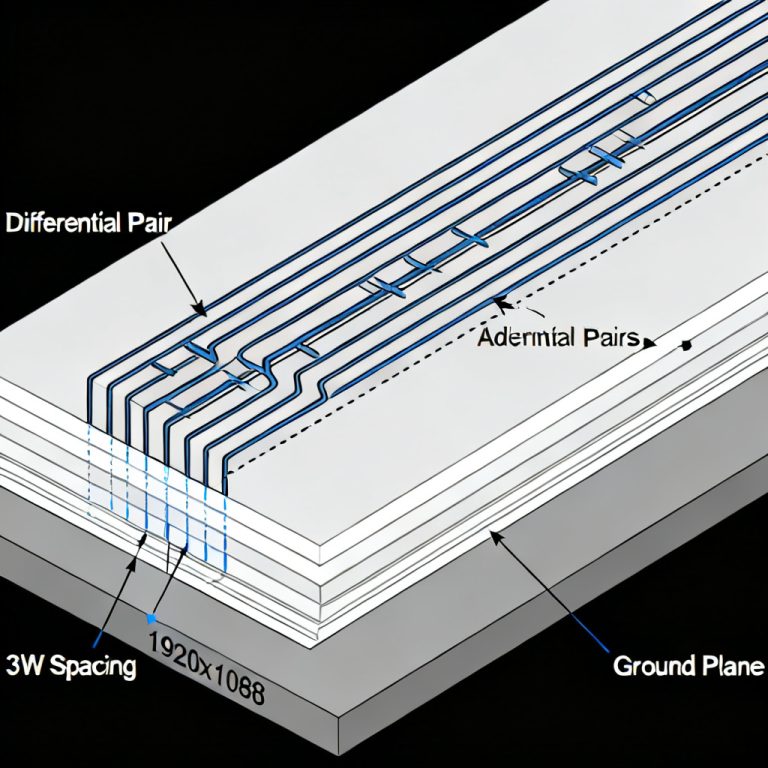
For Series Termination, add a resistor (e.g., 33Ω) at the source to match Z0, simulating with R in series. For Parallel Termination, add a resistor to ground (e.g., 50Ω) at the load, using Term with Z0 = 50Ω. For AC Termination, use a capacitor in series with a resistor for differential pairs.
6.3 Iterative Optimization
Use ADS Optimization: define goals such as S11 < -20 dB from 0 to 10 GHz or V_overshoot < 10%, and let ADS sweep trace width, stub length, or via parameters to meet the goal.
Step 7: Validating with Eye Diagram Analysis
7.1 Generate a PRBS Signal
Use PRBS source (e.g., 2^7-1 pattern, 10 Gbps). Add a Channel model (your transmission line with discontinuities).
7.2 Plot the Eye Diagram
In data display, use EyeDiagram function. A wide-open eye means low reflection (good signal integrity). A closed eye with jitter means significant reflection. If your TDR shows a 5Ω impedance bump, your eye diagram will show approximately 15% eye closure at 10 Gbps.
Step 8: Common Pitfalls and Best Practices for Reflection in Transmission Line Simulation in Keysight ADS
| Pitfall | Solution |
|---|---|
| Using ideal models only | Always include via, connector, and stackup models from your PCB manufacturer. |
| Ignoring skin effect at high frequencies | Use S-Parameter models with frequency-dependent loss (e.g., W-element). |
| Not simulating multiple corners | Run simulation with +10% tolerance on Z0 and Er. |
| Forgetting source reflection | Add a 50Ω source impedance (Rs=50Ω) to avoid infinite reflections. |
Frequently Asked Questions about Reflection in Transmission Line Simulation in Keysight ADS
What is the reflection coefficient in transmission line simulation?
The reflection coefficient (Γ) in Reflection in Transmission Line Simulation in Keysight ADS is defined as Γ = (Z_load – Z_0) / (Z_load + Z_0), measuring the amount of signal reflected due to impedance mismatch.
How do I simulate TDR in Keysight ADS for reflection analysis?
In Reflection in Transmission Line Simulation in Keysight ADS, after S-parameter simulation, use the TDR function: TDR = tdr(S11, 50, time) to obtain the impedance profile.
What causes signal reflection in high-speed PCB designs?
Signal reflection in high-speed PCB designs is caused by impedance discontinuities such as vias, bends, connectors, or changes in trace width, which are analyzed through Reflection in Transmission Line Simulation in Keysight ADS.
Conclusion: From Simulation to Manufacturable High-Speed PCBs
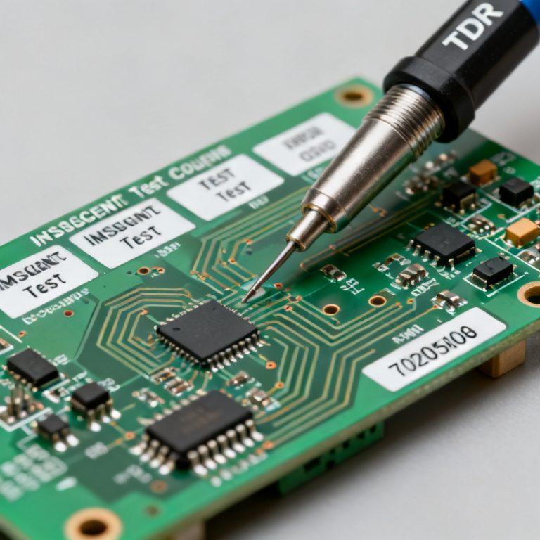
Reflection in Transmission Line Simulation in Keysight ADS is the bridge between theoretical design and a working PCB. By following this step-by-step guide, you can ensure that your high-speed designs achieve less than -15 dB return loss and greater than 0.7 UI eye opening. As a B2B PCB manufacturer specializing in high-speed boards, we use these exact ADS workflows to validate every design before fabrication. We provide impedance-controlled stackups (50Ω ±5%), TDR test coupons on every panel, and simulation-to-fabrication correlation reports. Contact us for a free ADS simulation review and PCB quote.