Master eye diagram PCB measurements for high-speed designs. This guide covers oscilloscope setup, jitter decomposition, and compliance testing for signal integrity.
Eye Diagram PCB Measurements: Fundamentals You Must Know
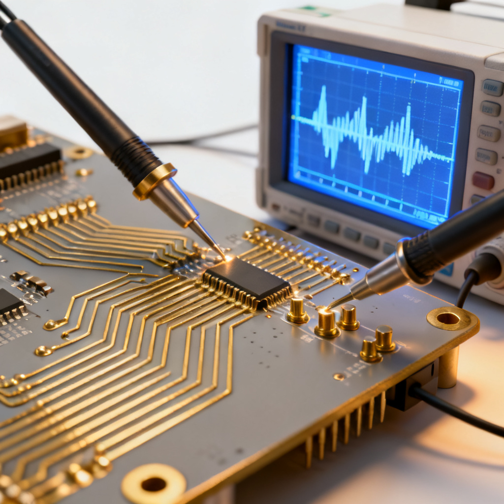
An eye diagram PCB measurement overlays multiple bits of a digital signal triggered by a clock or data pattern. Key metrics include eye height (voltage margin), eye width (timing margin), rise/fall time, jitter, and eye mask compliance.
Insight from Keysight: Eye diagrams diagnose root causes of signal degradation like reflections, crosstalk, or power supply noise. For high-speed PCBs, issues often stem from via stubs, trace discontinuities, or insufficient ground planes.
Rohde & Schwarz: Oscilloscope and probe bandwidth must be at least 3–5 times the fundamental frequency. For 10 Gbps (5 GHz fundamental), a 25–50 GHz bandwidth is recommended. Insufficient bandwidth artificially closes the eye.
Analog Devices: Eye diagrams are statistical; a single-shot capture is insufficient. Real-time oscilloscopes capture all bits in one trigger event, unlike sampling oscilloscopes which require repetitive patterns.
Eye Diagram and Signal Integrity Basics
Eye diagram PCB measurements reveal amplitude noise, timing jitter, and intersymbol interference (ISI). For B2B PCB manufacturers, passing eye mask tests (PCIe, USB, Ethernet) is critical.
Hardware Setup for Eye Diagram PCB Measurements
Oscilloscope Selection
Real-time vs. sampling: For non-repetitive signals (PRBS patterns), a real-time oscilloscope is mandatory. Bandwidth rule (Keysight & Rohde & Schwarz): Bandwidth ≥ 5 × Data Rate. For 10 Gbps, at least 50 GHz. Sample rate ≥ 2.5× bandwidth. Deep memory (2 Gpts) captures long patterns for low-probability jitter events.
Probing Strategy
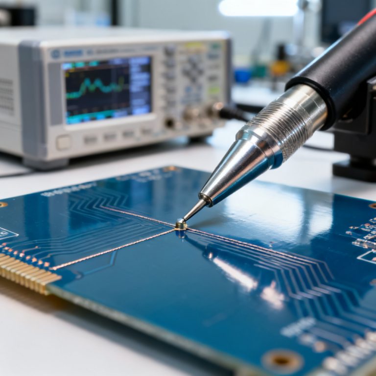
Differential probing (all sources): Use a differential probe with bandwidth matching the oscilloscope. Minimize capacitive loading (<0.3 pF). Solder-in coaxial cable or precision probe tip directly to PCB test point. Avoid handheld probes for high-speed signals.
Access points: Place SMA connectors or micro-coaxial test points near the receiver (RX) pads.
Cable and Connection Quality
Use low-loss coaxial cables (2.92 mm or 1.85 mm connectors for >40 GHz). Keep cable lengths under 1 meter. Analog Devices notes that poor connections can introduce 1–2 ps of jitter.
Step-by-Step Oscilloscope Configuration for Eye Diagram PCB Measurements
Step 1: Connect and Calibrate
Power on and warm up for 30 minutes. Perform self-calibration (deskew) of all channels (Keysight recommends <1 ps delay matching). Connect probe and set to differential mode.
Step 2: Set Up Clock Recovery
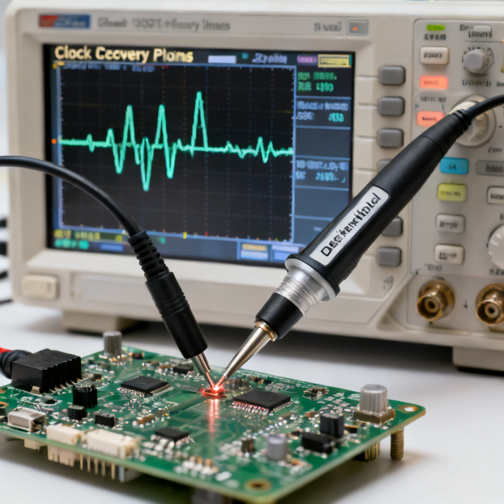
Use a Phase-Locked Loop (PLL) with loop bandwidth matching the standard (e.g., 10 MHz for PCIe Gen3). For compliance, use “Golden PLL” parameters. Rohde & Schwarz: Enable hardware clock recovery for real-time tracking. Analog Devices: If signal has excessive jitter, reduce PLL bandwidth.
Step 3: Configure Triggering
Trigger source: data signal (if clock recovery enabled) or separate clock. Trigger level at midpoint (50% of Vpp). For differential signals, trigger on zero crossing. Use “Eye Trigger” mode if available.
Step 4: Acquire the Waveform
Set timebase to 2–4 UI per division. Vertical scale so signal occupies 80% of screen. Press “Run”. The scope overlays bits to form the eye.
Step 5: Optimize Eye Display
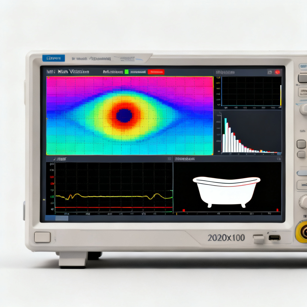
Set persistence to “Infinite” or “Long” (Rohde & Schwarz: at least 10,000 acquisitions). Enable color-graded persistence (heat map). Load eye mask template for your protocol.
Advanced Analysis: Jitter and Noise in Eye Diagram PCB Measurements
Eye Mask Testing
Keysight: Use “Mask Margin” measurement. Margin >20% is good; <10% requires design changes. Rohde & Schwarz: For automated compliance (USB 3.0), use built-in test suite.
Jitter Decomposition
Jitter is critical for high-speed PCBs. Random Jitter (RJ) is Gaussian; Deterministic Jitter (DJ) is bounded. Total Jitter (TJ) = DJ + 14.1×RJ (BER=1e-12).
How to measure: Use scope’s jitter analysis software (Keysight EZJIT, Rohde & Schwarz Jitter Analysis, Analog Devices VisualAnalog). Select TIE (Time Interval Error) plot. Apply FFT to TIE plot to identify periodic jitter. Separate RJ and DJ using histogram. Analog Devices: Capture at least 1 million bits for accurate RJ.
Noise and Amplitude Analysis
Eye height: vertical opening at center. Bathtub curve: BER vs. sampling phase (width at BER=1e-12 is eye opening). Rise/fall time: 20%/80% thresholds; slow edges indicate driver issues or capacitance.
Troubleshooting Common Eye Diagram PCB Measurement Issues
Problem 1: Eye Completely Closed
Cause: No signal, clock recovery failure, probe not connected. Fix: Check probe, verify data rate, ensure PLL lock.
Problem 2: Eye Open but Mask Violations
Cause: Excessive jitter (DJ from ISI) or noise. Fix: Reduce trace length, add equalization (CTLE/DFE), improve decoupling, use lower-loss PCB material (Rogers 4350B).
Problem 3: Asymmetric Eye
Cause: Duty cycle distortion (DCD), skew in differential pair. Fix: Check driver symmetry; match differential trace lengths within 5 mils.
Problem 4: Multiple Eyes (Ghosting)
Cause: Reflections from impedance discontinuities (vias, connectors). Fix: Use impedance-controlled routing (50Ω single-ended, 100Ω differential), back-drill vias, correct termination.
Problem 5: Jitter Peaks at Specific Frequencies
Cause: Periodic jitter from switching power supply ripple or clock harmonic. Fix: Add ferrite beads, spread-spectrum clocking, increase PLL bandwidth.
PCB Design Best Practices for Better Eye Diagram PCB Measurements
1. Stackup: Symmetrical with continuous ground planes. Minimize dielectric thickness. 2. Trace routing: Tightly coupled differential pairs, avoid 90° bends. 3. Via management: Back-drill high-speed vias; limit stub length <10 mils. 4. Power integrity: Decoupling capacitors within 50 mils of IC pins. 5. Termination: Match driver impedance to trace impedance (50Ω series, 100Ω differential). 6. Test points: Dedicated SMA connectors near receiver.
Why Our High-Speed PCB Manufacturing Ensures Reliable Eye Diagram Measurements
We combine advanced stackup design, precise impedance control, and rigorous test coupon validation. Our DFM team optimizes your design for manufacturing, ensuring eye mask compliance from 1 Gbps to 100 Gbps. Unlike generic fabricators, we provide full signal integrity reports with every prototype.
| Parameter | Typical Value (10 Gbps) | Measurement Tool |
|---|---|---|
| Eye Height (voltage margin) | >300 mV | Real-time oscilloscope |
| Eye Width (timing margin) | >0.6 UI | Jitter analysis software |
| Total Jitter (BER=1e-12) | <30 ps | TIE histogram |
| Rise/Fall Time (20%–80%) | <25 ps | Oscilloscope measurement |
Frequently Asked Questions about Eye Diagram PCB Measurements
What is an eye diagram in PCB measurements?
An eye diagram PCB measurement overlays multiple bits of a digital signal to visualize signal quality, revealing noise, jitter, and intersymbol interference. It is essential for high-speed PCB validation.
How do I set up an eye diagram with a real-time oscilloscope?
Configure clock recovery (PLL), set trigger level at 50% amplitude, acquire waveform with persistence, and load eye mask. Use bandwidth ≥5× data rate for accurate eye diagram PCB measurements.
What causes a closed eye diagram?
Common causes: excessive jitter (ISI, crosstalk), impedance mismatches, power supply noise, or insufficient oscilloscope bandwidth. Troubleshoot using jitter decomposition and TDR analysis.
Key Terminology for Eye Diagram PCB Measurements
- ISI (Intersymbol Interference): Distortion caused by previous bits affecting current bit, common in long traces.
- PLL (Phase-Locked Loop): Circuit used for clock recovery; loop bandwidth critical for jitter tracking.
- TIE (Time Interval Error): Deviation of edge timing from ideal clock; used for jitter analysis.
- Bathtub Curve: Plot of BER vs. sampling phase; width at target BER defines eye opening.