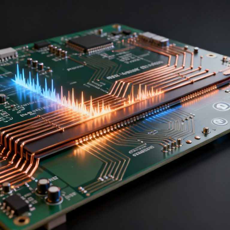
In the world of high-speed PCB design, Random Jitter in High Speed PCB sets the ultimate performance limit for serial links. Unlike deterministic jitter, random jitter is Gaussian, unbounded, and fundamentally irreducible, stemming from thermal noise and flicker noise within components.
Fundamentals of Random Jitter in High Speed PCB
What is Random Jitter in High Speed PCB?
Random jitter in high speed PCB refers to the timing uncertainty of a signal edge caused by stochastic, noise-driven processes. It is characterized by its Gaussian probability density function (PDF). This means the jitter amplitude is unbounded; theoretically, a jitter event can be of any size, though the probability decreases exponentially with amplitude.
Key Characteristics of Random Jitter
- Unbounded: The peak-to-peak value increases indefinitely as the measurement time increases (e.g., a 10⁻¹² bit error rate requires a peak-to-peak value of approximately 14 times the RMS value).
- Uncorrelated: It has no relationship with the data pattern or the bit rate.
- Additive: Its RMS value adds in a root-sum-square (RSS) fashion with other independent noise sources.
- Gaussian Distribution: Measured in RMS (root mean square) values, typically in picoseconds.
The Impact on High-Speed Links
In a high-speed serial link, the total jitter budget is allocated between the transmitter, channel, and receiver. Random jitter in high speed PCB is particularly dangerous because it cannot be tracked by a clock-data recovery (CDR) circuit. While a CDR can track low-frequency wander (like that from some flicker noise), the high-frequency tail of the Gaussian distribution directly eats into the timing margin, causing bit errors. The industry-standard metric for this is the Total Jitter (TJ), often extrapolated to a Bit Error Rate (BER) of 10⁻¹², using the formula:
TJ(BER) = DJ(peak-to-peak) + 2 × Q × RJ(RMS)
Where Q is the factor corresponding to the target BER (e.g., Q ≈ 14 for BER 10⁻¹²).
Thermal Noise: The Fundamental Floor for Random Jitter in High Speed PCB
Thermal noise is the most fundamental and inescapable source of random jitter in high speed PCB design.
The Physics of Thermal Noise
Thermal noise, also known as Johnson-Nyquist noise, is generated by the random thermal agitation of charge carriers (electrons) within a conductor. This agitation creates a fluctuating voltage, even in the absence of an applied current.
- Origin: The random, Brownian motion of electrons in resistors, PCB traces, and the channel of a transistor.
- Characteristics:
- White Noise Spectrum: Its power spectral density is flat across all frequencies (up to the terahertz range).
- Temperature Dependent: The noise power is directly proportional to absolute temperature (T).
- Resistance Dependent: The noise voltage is proportional to the square root of the resistance (R).
The RMS noise voltage generated across an open-circuit resistor is given by:
Vn = √(4 × kB × T × R × Δf)
Where kB is Boltzmann’s constant (1.38 × 10⁻²³ J/K), T is the absolute temperature in Kelvin, R is the resistance in Ohms, and Δf is the bandwidth in Hz.
How Thermal Noise Becomes Jitter
Thermal noise does not directly create jitter in a pure digital signal. It becomes jitter when a noisy signal crosses a threshold (e.g., the input of a buffer, a comparator, or a clock driver). Consider a clock signal with a finite slew rate (SR). A voltage noise (Vn) on the signal edge will cause a timing uncertainty (tj) proportional to the noise voltage divided by the slew rate: tj = Vn / SR.
Implications for PCB Design
- Low Slew Rates are Vulnerable: A slow-rising clock edge is far more susceptible to thermal noise-induced jitter than a fast edge. This is why high-speed designs demand fast edge rates.
- Impedance and Loss: The resistance of a PCB trace (which increases with frequency due to the skin effect) directly contributes to thermal noise. Longer, lossy traces generate more noise.
- Termination Resistors: While necessary for impedance matching, on-die termination (ODT) resistors are a direct source of thermal noise. A 50-ohm termination resistor at room temperature in a 10 GHz bandwidth generates approximately 90 µV RMS of noise.
Mitigation Strategies for Thermal Noise
- Minimize Resistance: Use wider traces for critical clock and data lines to reduce DC resistance. Use low-resistance materials (e.g., thicker copper).
- Increase Slew Rate: Use drivers with faster edge rates on critical paths. This is a trade-off against EMI, but for internal routing, it is highly effective.
- Reduce Bandwidth: Use low-pass filtering on the power supply and signal paths to limit Δf. However, this cannot be done on the data signal itself without destroying the signal.
- Lower Temperature: While often outside the designer’s direct control, proper thermal management (heat sinks, airflow) reduces thermal noise.
- Use Low-Noise Components: Select oscillators, PLLs, and buffers with low phase noise specifications.
Flicker Noise: The Low-Frequency Drifter in Random Jitter in High Speed PCB
While thermal noise sets the broadband floor, flicker noise dominates at low frequencies and is a major contributor to close-in phase noise in oscillators and PLLs, directly affecting random jitter in high speed PCB.
The Physics of Flicker Noise
Flicker noise, also known as 1/f noise or pink noise, is a low-frequency phenomenon whose origin is less fundamental than thermal noise but is universally observed in all active devices and some passive components.
- Origin: The exact physical cause is still debated, but it is widely attributed to traps and defects in the semiconductor crystal lattice. Charge carriers are randomly captured and released by these traps, causing fluctuations in current.
- Characteristics:
- Pink Noise Spectrum: Its power spectral density is inversely proportional to frequency (1/f^α), where α is typically close to 1.
- DC Current Dependent: The noise power is proportional to the square of the DC bias current (I²).
- Device Dependent: CMOS devices generally have higher flicker noise than bipolar junction transistors (BJTs).
How Flicker Noise Becomes Jitter
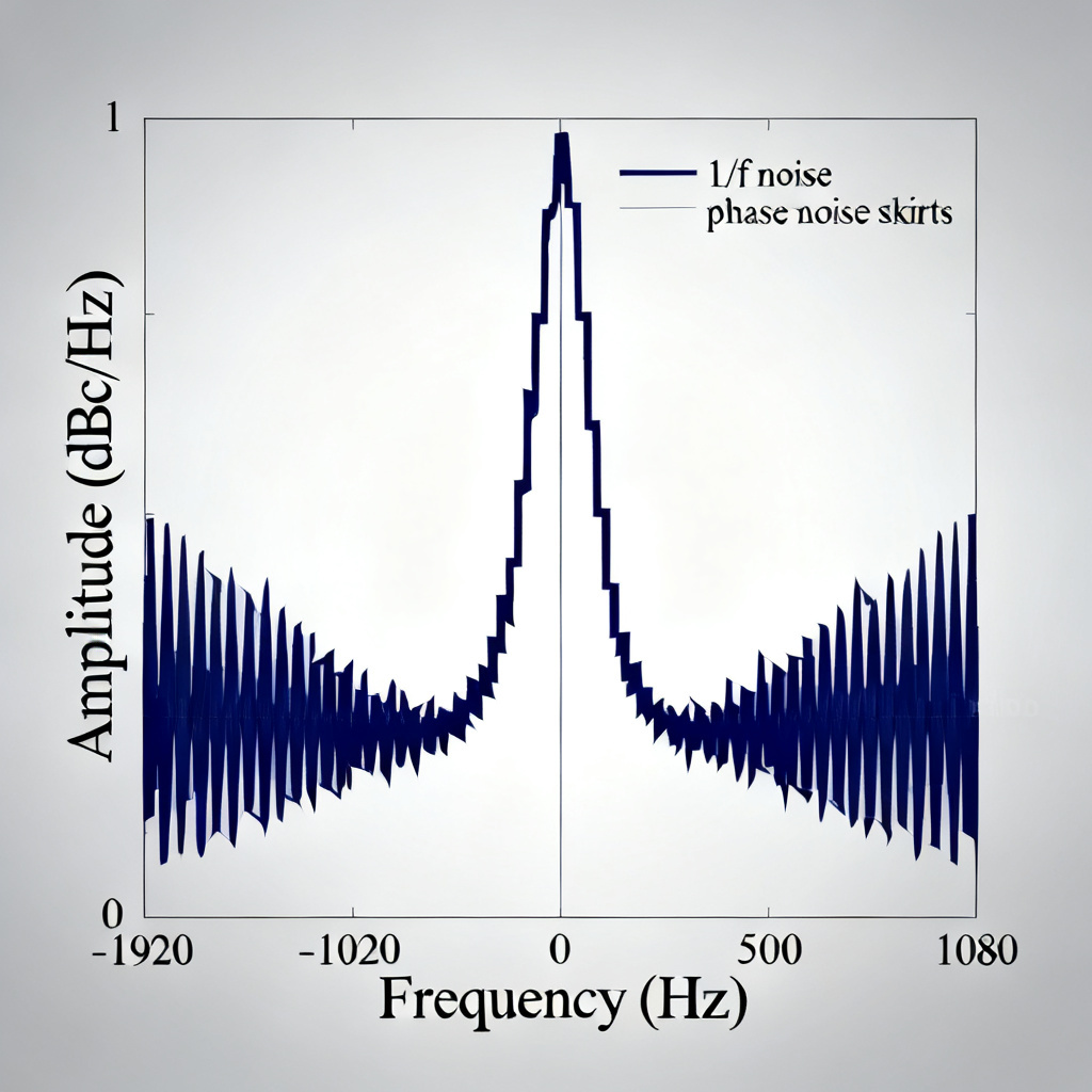
Flicker noise is the dominant source of phase noise in oscillators at small frequency offsets (e.g., 1 kHz to 1 MHz). It modulates the phase of the carrier signal, creating “wander” or slow drift in the zero-crossing points.
- In Oscillators: Flicker noise in the transistor of an oscillator circuit is up-converted to phase noise around the carrier frequency. This creates “skirts” of noise around the fundamental frequency.
- In PLLs: The flicker noise of the phase detector, charge pump, and VCO contributes to the integrated phase noise of the PLL output. This low-frequency jitter is often tracked by the CDR, but its residual effect still contributes to the overall jitter budget.
- In Active Components: Buffers, line drivers, and clock distribution chips all have flicker noise that modulates their propagation delay, creating jitter on the output clock.
Key Differences: Thermal Noise vs. Flicker Noise
| Feature | Thermal Noise | Flicker Noise |
|---|---|---|
| Spectrum | White (flat) | Pink (1/f) |
| Dominant Frequency | High frequencies (broadband) | Low frequencies (near DC) |
| Primary Source | Resistors, traces, channel | Transistors (CMOS > BJT) |
| Dependence | Resistance, Temperature | DC Current, Device Physics |
| Impact on Jitter | High-frequency, unbounded tail | Low-frequency wander, phase noise |
| Mitigation | Fast slew rates, low R | Large device area, bias current |
Mitigation Strategies for Flicker Noise
- Component Selection: This is the most critical step. Choose oscillators and clock generators with specified low phase noise at low frequency offsets (e.g., 10 Hz, 100 Hz, 1 kHz). Look for components using SiGe or GaAs processes, which typically have lower 1/f noise than standard CMOS.
- Device Geometry: In integrated circuit design, flicker noise is inversely proportional to the gate area of a transistor. Using larger transistors reduces 1/f noise. For PCB designers, this means selecting “low noise” or “ultra-low noise” ICs.
- Bias Current Optimization: There is a sweet spot for bias current. Too little current increases the impact of flicker noise; too much current increases thermal noise. Follow the manufacturer’s recommendations for optimal bias.
- AC Coupling: For circuits where the DC level is not critical, AC coupling can remove the low-frequency drift caused by flicker noise. This is common in high-speed serial links.
- Clean Power Supply: Flicker noise in a VCO is exacerbated by noisy power supplies. Use dedicated, low-noise LDOs and extensive decoupling for PLL and oscillator power pins.
Advanced Insights and Practical Measurement for Random Jitter in High Speed PCB
The Corner Frequency (fc)
A crucial concept is the “flicker corner frequency,” the frequency at which the flicker noise power spectral density equals the thermal noise floor. Below fc, flicker noise dominates; above it, thermal noise dominates.
- For a typical CMOS transistor: fc can be in the range of 1 kHz to 1 MHz.
- For a BJT: fc is typically lower, from 10 Hz to 1 kHz.
- For a precision resistor: fc is extremely low (sub-1 Hz), so thermal noise dominates for all practical purposes.
Implication: When designing a high-speed link, the total integrated jitter is a combination of the thermal noise (broadband) and the flicker noise (low-frequency). The CDR’s loop bandwidth determines how much of the low-frequency jitter is tracked. A wider loop bandwidth tracks more flicker noise, reducing its impact on the total jitter at the receiver.
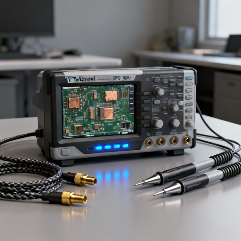
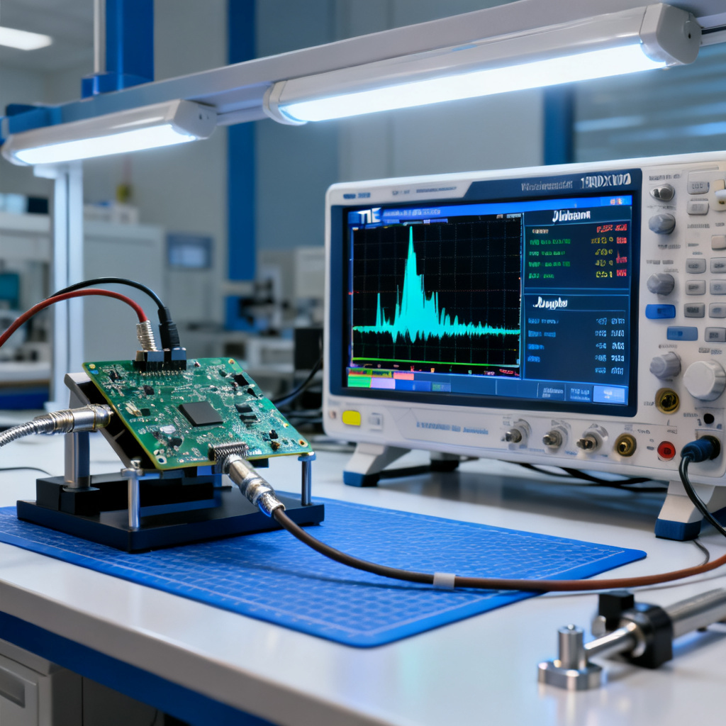
Measuring Random Jitter
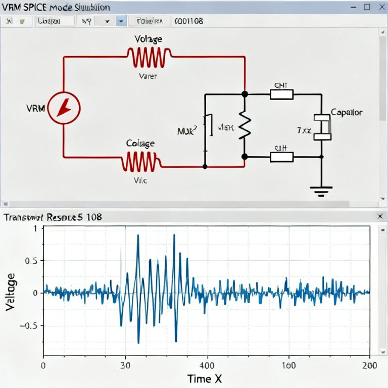
Separating RJ from DJ in a measurement is a specialized task. The most common method is using a Time Interval Analyzer (TIA) or a Real-Time Oscilloscope with jitter analysis software.
- Histogram Method: A histogram of the time interval error (TIE) is collected. The distribution is fitted to a dual-Dirac model. The standard deviation of the Gaussian tails of the histogram is the RMS random jitter.
- Spectral Method: The TIE data is converted to the frequency domain using an FFT. The flat portion of the phase noise spectrum (away from the carrier) represents the thermal noise contribution. The 1/f slope near the carrier represents the flicker noise contribution.
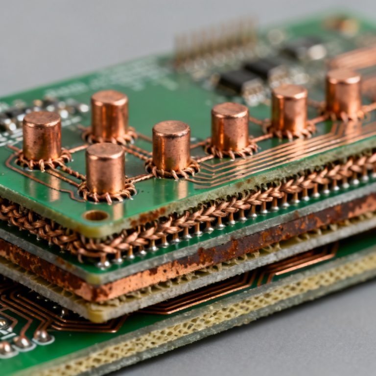
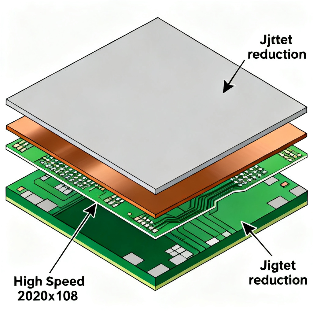
The Role of the PCB Stackup
The PCB itself is a source of thermal noise. The “loss tangent” of the dielectric material contributes to the AC resistance of the trace.
- Low-Loss Materials: Using high-frequency laminates (e.g., Rogers, Isola, Megtron) with a low dissipation factor (Df) reduces the trace’s AC resistance, thereby reducing thermal noise.
- Surface Roughness: The rough copper surface at the interface with the dielectric increases the effective resistance due to the skin effect, particularly at high frequencies. This adds to the thermal noise. Smoother copper foils (e.g., VLP, HVLP) are beneficial for extremely high-speed designs.
Conclusion: A Holistic Approach to Noise Management
Random jitter is an unavoidable physical reality in high-speed PCB design. It is not a “bug” but a feature of the universe’s thermodynamics and quantum mechanics. The key to successful design is not to eliminate it—that is impossible—but to manage its sources and minimize its impact.
Final Checklist for the High-Speed PCB Designer
- Prioritize Slew Rate: For all critical clock and data signals, use the fastest edge rate your system can tolerate without creating excessive EMI.
- Select Low-Noise Components: This is your single most powerful tool. Invest in high-quality oscillators, PLLs, and clock buffers with published phase noise specifications. Do not rely solely on “jitter” specs; look at the phase noise plot.
- Minimize Trace Resistance: Use wider traces and shorter lengths for critical paths. Choose low-loss PCB materials for multi-gigabit designs.
- Design for Low Power Supply Noise: Use dedicated, low-noise LDOs for all sensitive analog and clocking circuits. Implement a robust decoupling strategy.
- Understand Your CDR: Know the bandwidth of your receiver’s clock-data recovery circuit. This determines how much low-frequency jitter (flicker noise) is tolerated.
FAQ: Random Jitter in High Speed PCB
What is the primary difference between thermal noise and flicker noise in high speed PCB?
Thermal noise in high speed PCB is white noise generated by random electron agitation in conductors, while flicker noise is 1/f noise caused by traps in semiconductor devices. Thermal noise dominates at high frequencies; flicker noise dominates at low frequencies.
How does random jitter in high speed PCB affect bit error rate?
Random jitter in high speed PCB creates an unbounded Gaussian timing uncertainty. At a target BER of 10⁻¹², the peak-to-peak jitter is approximately 14 times the RMS jitter, directly reducing the timing margin and causing bit errors.
Can random jitter in high speed PCB be completely eliminated?
No, random jitter in high speed PCB cannot be completely eliminated because thermal noise is a fundamental physical phenomenon. However, it can be minimized through proper component selection, fast slew rates, low-resistance traces, and clean power supply design.
What is the flicker corner frequency in high speed PCB?
The flicker corner frequency is the point where flicker noise power equals thermal noise power. Below this frequency, flicker noise dominates random jitter in high speed PCB; above it, thermal noise dominates. For CMOS devices, this is typically 1 kHz to 1 MHz.
How does PCB stackup impact random jitter in high speed PCB?
PCB stackup impacts random jitter in high speed PCB through trace resistance and dielectric loss. Low-loss materials (low Df) and smooth copper foils reduce AC resistance, thereby reducing thermal noise contribution to random jitter.