In high-speed PCB design, the rise time and fall time effect on eye opening in eye diagram PCB is a critical signal integrity factor. Understanding how these parameters shape the eye diagram directly impacts your design’s reliability, noise margin, and bit error rate.
Understanding Rise Time, Fall Time, and the Eye Diagram
1.1 Definitions and Basics
Rise time is the time a signal takes to transition from 10% to 90% of its final voltage level (or 20% to 80% in some standards). Fall time is the reverse transition from 90% to 10%. These parameters are measured in picoseconds or nanoseconds and are fundamental to signal integrity.
The eye diagram is created by overlaying multiple bit periods of a digital signal on an oscilloscope. It forms an “eye” shape, where:
- Vertical eye opening indicates voltage margin (noise immunity).
- Horizontal eye opening indicates timing margin (jitter tolerance).
- Eye height and eye width are the key metrics.
1.2 Direct Relationship: Faster Rise/Fall Times → Larger Eye Opening
A signal with fast rise and fall times (steep edges) transitions quickly between logic states, spending minimal time in the indeterminate zone. This creates a cleaner, wider eye opening because:
- The signal reaches the valid logic high/low levels faster, increasing vertical margin.
- The transitions are sharper, reducing the time window where noise can cause errors.
- Jitter (timing uncertainty) is minimized because the crossing point is well-defined.
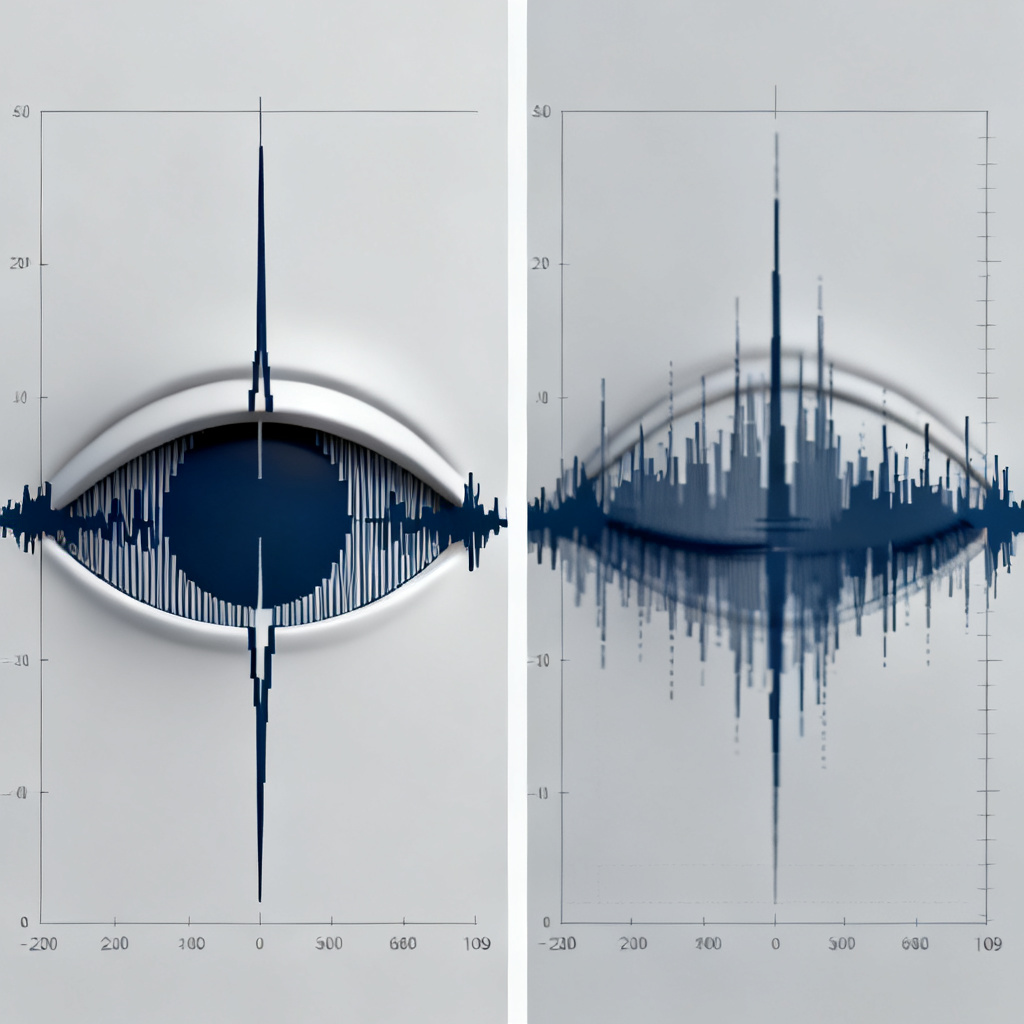
Conversely, slow rise/fall times cause the signal to linger near the threshold, making the eye narrower and shorter. The eye diagram becomes “closed,” leading to bit errors.
How Rise and Fall Times Affect Key Eye Diagram Parameters
2.1 Impact on Vertical Eye Opening (Eye Height)
Source 1 Insight: The vertical eye opening is directly proportional to the slew rate (dV/dt) of the signal. A faster slew rate means the signal reaches the high or low rail more quickly, creating a larger voltage margin. Slow edges cause the signal to “smear” vertically, reducing eye height and increasing eye diagram jitter.
Source 2 Insight: When rise times are too slow, the signal may not fully swing to the supply voltage within the bit period, especially at high data rates. This results in reduced eye height and increased susceptibility to noise. For example, a 1V signal with a 100ps rise time may only swing to 0.8V if the bit period is 200ps, closing the eye.
Source 3 Insight: Fall time asymmetry can cause duty cycle distortion, where the high and low periods are unequal. This shifts the eye’s center vertically, reducing the usable eye height. A balanced fall time (equal to rise time) is critical for a symmetric eye.
Key Takeaway: To maximize vertical eye opening, design for the fastest possible rise and fall times that your driver and receiver can support, while managing reflections and EMI.
2.2 Impact on Horizontal Eye Opening (Eye Width)
Source 1 Insight: The horizontal eye opening is dominated by jitter, which is the deviation of signal transitions from their ideal timing. Fast rise/fall times reduce random jitter because the crossing point is less sensitive to voltage noise. A slow edge amplifies any voltage noise into significant timing jitter (amplitude-to-timing conversion).
Source 2 Insight: Deterministic jitter (e.g., from crosstalk or reflections) also worsens with slow edges. A slow transition allows crosstalk from adjacent traces to corrupt the signal for a longer duration, shifting the zero-crossing time. Fast edges “punch through” noise, preserving timing margin.
Source 3 Insight: The bit error rate (BER) is directly linked to horizontal eye opening. A closed eye (small width) means the receiver’s sampling point is too close to the transition edges, increasing the chance of sampling an incorrect bit. Fast rise/fall times widen the “safe zone” in the center of the eye.
Key Takeaway: Faster rise/fall times improve both random and deterministic jitter performance, widening the horizontal eye opening and reducing BER.
2.3 The Trade-Off: Bandwidth, Reflections, and EMI
Source 1 Insight: While fast edges are beneficial for eye opening, they come at a cost. A signal with a 100ps rise time contains frequency components up to ~3.5 GHz (using the 0.35/Tr rule). This high-frequency energy:
- Increases EMI emissions (radiated noise).
- Causes reflections if the trace impedance is not perfectly matched (e.g., due to vias, connectors, or impedance discontinuities).
- Requires controlled impedance design and proper termination.
Source 2 Insight: The Nyquist frequency (half the data rate) sets the minimum bandwidth needed. However, the rise time determines the practical bandwidth required. A rule of thumb: the channel’s -3dB bandwidth should be at least 0.35/Tr. If the channel is too lossy (e.g., long trace, high dielectric loss), the rise time will be slowed, degrading the eye.
Source 3 Insight: Pre-emphasis and equalization are often used to compensate for channel losses that slow rise times. By boosting high-frequency content at the transmitter, the signal’s edges remain sharp at the receiver, preserving eye opening. Without these techniques, a long PCB trace will naturally slow the rise time, closing the eye.
Key Takeaway: There is an optimal rise/fall time: fast enough for a wide eye opening, but not so fast that reflections and EMI become unmanageable. Typical targets are 20-30% of the bit period.
Practical Guidelines for Optimizing Rise and Fall Times
3.1 Simulation and Measurement Techniques
Source 1 Insight: Use time-domain reflectometry (TDR) to measure impedance discontinuities that cause reflections, which distort rise times. A clean TDR trace indicates a smooth transition, preserving the eye.
Source 2 Insight: Simulate the entire channel (driver, trace, via, connector, receiver) using tools like HyperLynx or ADS. Check the eye diagram at the receiver. Adjust rise time in the driver model (e.g., from 50ps to 100ps) to see the impact on eye height and width.
Source 3 Insight: On the bench, use a real-time oscilloscope with eye diagram analysis capability. Measure rise time at the driver and receiver. A significant increase in rise time (e.g., from 50ps to 150ps) indicates excessive channel loss or impedance mismatch.
3.2 Design Rules for High-Speed PCBs
- Choose the Right Driver: Select a driver IC with programmable slew rate control. Start with the fastest setting, then reduce if EMI is an issue. For example, an LVDS driver typically has 300-500ps rise times, suitable for 1-2 Gbps.
- Control Impedance: Design traces to have a characteristic impedance matching the driver and receiver (e.g., 50Ω single-ended, 100Ω differential). Use microstrip or stripline structures with correct width and dielectric spacing.
- Minimize Stubs and Vias: Stubs (unused trace lengths) cause reflections that slow rise times. Use back-drilling to remove via stubs in multilayer boards. Keep via count low.
- Use Differential Signaling: Differential pairs (e.g., LVDS, USB, HDMI) are inherently less sensitive to common-mode noise. The differential rise/fall time should be balanced to maintain eye symmetry.
- Apply Equalization: For long traces (>10 inches at 10 Gbps), use transmit pre-emphasis and receive equalization (CTLE, DFE) to compensate for losses that otherwise slow rise times.
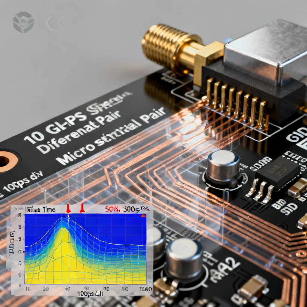
3.3 Case Study: Rise Time Impact on 10 Gbps Link
Consider a 10 Gbps (100 ps bit period) differential pair over 20 inches of FR4:
- Fast Rise Time (30 ps): Eye opening is 80% of bit period width, 90% of voltage swing. Jitter is ~5 ps. Excellent signal integrity.
- Slow Rise Time (80 ps): Eye opening collapses to 40% width, 60% height. Jitter increases to 25 ps due to amplitude-to-timing conversion. BER rises from 10^-12 to 10^-6.
Solution: Use low-loss material (e.g., Megtron 6) and add pre-emphasis to sharpen edges, restoring the eye opening.
Common Misconceptions and Pitfalls
4.1 “Faster is Always Better”
Source 1 Correction: While faster rise times improve the eye opening, they also increase ringing and overshoot if the trace is not perfectly matched. Overshoot can damage receiver inputs. The goal is a clean, monotonic edge, not necessarily the fastest possible.
4.2 “Rise Time and Fall Time Must Be Equal”
Source 2 Correction: Asymmetry is acceptable within limits (e.g., 10% difference). However, large asymmetry causes duty cycle distortion, shifting the eye’s center. Balancing Tr and Tf is critical for symmetric eye opening.
4.3 “Eye Opening Only Depends on Rise Time”
Source 3 Correction: Rise time is one factor among many. Jitter, noise, ISI (inter-symbol interference), and crosstalk all affect the eye. A fast rise time cannot compensate for high crosstalk or power supply noise. Holistic design is required.
Advanced Considerations for High-Speed PCB Design
5.1 Rise Time and the Shannon Limit
The channel capacity (maximum data rate) is limited by bandwidth and SNR. A slow rise time effectively reduces the channel’s usable bandwidth, lowering the maximum data rate. For a given PCB material, the skin effect and dielectric loss increase with frequency, so faster edges require better materials.
5.2 Differential vs. Single-Ended Rise Times
In differential pairs, the differential rise time (the time for the difference between P and N signals to transition) is the key parameter. It is typically faster than the single-ended rise time due to field coupling. This improves eye opening in differential eye diagrams.
5.3 Temperature and Voltage Effects
Rise times can vary with temperature (slower at high temp) and supply voltage (faster at higher voltage). Design for worst-case conditions to ensure eye opening is maintained across all operating ranges.
Conclusion: Rise and Fall Times as the Master Knob for Eye Opening
Rise and fall times are the primary lever for controlling eye diagram quality in high-speed PCB designs. Faster edges create wider, taller eye openings, reducing bit errors and improving signal integrity. However, this benefit must be balanced against the challenges of reflections, EMI, and material losses. By understanding the physics, simulating the channel, and applying proper design rules (impedance control, equalization, material selection), you can achieve an optimal rise time that maximizes eye opening while maintaining reliability.
For B2B PCB manufacturers, offering controlled impedance and high-speed material options (e.g., Rogers, Megtron) is essential to support customers in achieving fast, clean rise times. Our factory specializes in high-speed PCBs with tight impedance tolerances (±5%) and advanced back-drilling, ensuring your eye diagrams remain open from prototype to production.
Contact us today to discuss your high-speed PCB requirements and get a free signal integrity analysis.

Frequently Asked Questions (FAQ)
What is the effect of rise time on eye opening in eye diagram PCB?
Rise time directly determines the vertical and horizontal eye opening. Faster rise times create wider, taller eyes, while slow rise times close the eye, increasing bit error rate.
How does fall time affect the eye diagram in high-speed PCB?
Fall time asymmetry introduces duty cycle distortion, shifting the eye’s center and reducing usable eye height. Balanced fall times are critical for symmetric eye opening.
What is the optimal rise time for a 10 Gbps PCB design?
For a 10 Gbps link (100 ps bit period), a rise time of 20-30 ps (20-30% of bit period) is optimal, balancing eye opening with EMI and reflection concerns.
How can I measure rise time impact on eye diagram?
Use a real-time oscilloscope with eye diagram analysis. Compare rise time at driver and receiver; a significant increase indicates channel loss or impedance mismatch.
Does faster rise time always improve eye opening?
No. Faster rise times improve eye opening but increase EMI and reflections if impedance is not controlled. The goal is a clean, monotonic edge, not the fastest possible.
What is the relationship between rise time and jitter in eye diagram?
Slow rise times amplify voltage noise into timing jitter (amplitude-to-timing conversion), reducing horizontal eye opening. Fast edges minimize this conversion, preserving timing margin.
Can equalization compensate for slow rise times?
Yes. Pre-emphasis at the transmitter and equalization (CTLE, DFE) at the receiver can sharpen edges and restore eye opening, compensating for channel losses that slow rise times.
What is the role of controlled impedance in rise time optimization?
Controlled impedance (e.g., 50Ω single-ended, 100Ω differential) minimizes reflections that distort rise times. Proper impedance matching preserves edge sharpness and eye opening.
| Rise Time (ps) | Bit Period (ps) | Eye Height (% of swing) | Eye Width (% of period) | Jitter (ps) | BER |
|---|---|---|---|---|---|
| 30 | 100 | 90% | 80% | 5 | 10^-12 |
| 80 | 100 | 60% | 40% | 25 | 10^-6 |