In high-speed PCB design, vias create a gap in return path continuity, degrading signal integrity. This article explains how vias disrupt the return path and provides expert solutions for reliable B2B PCB manufacturing.

How Vias Create a Gap in the Return Path PCB Design
The Physics of Return Path Discontinuity
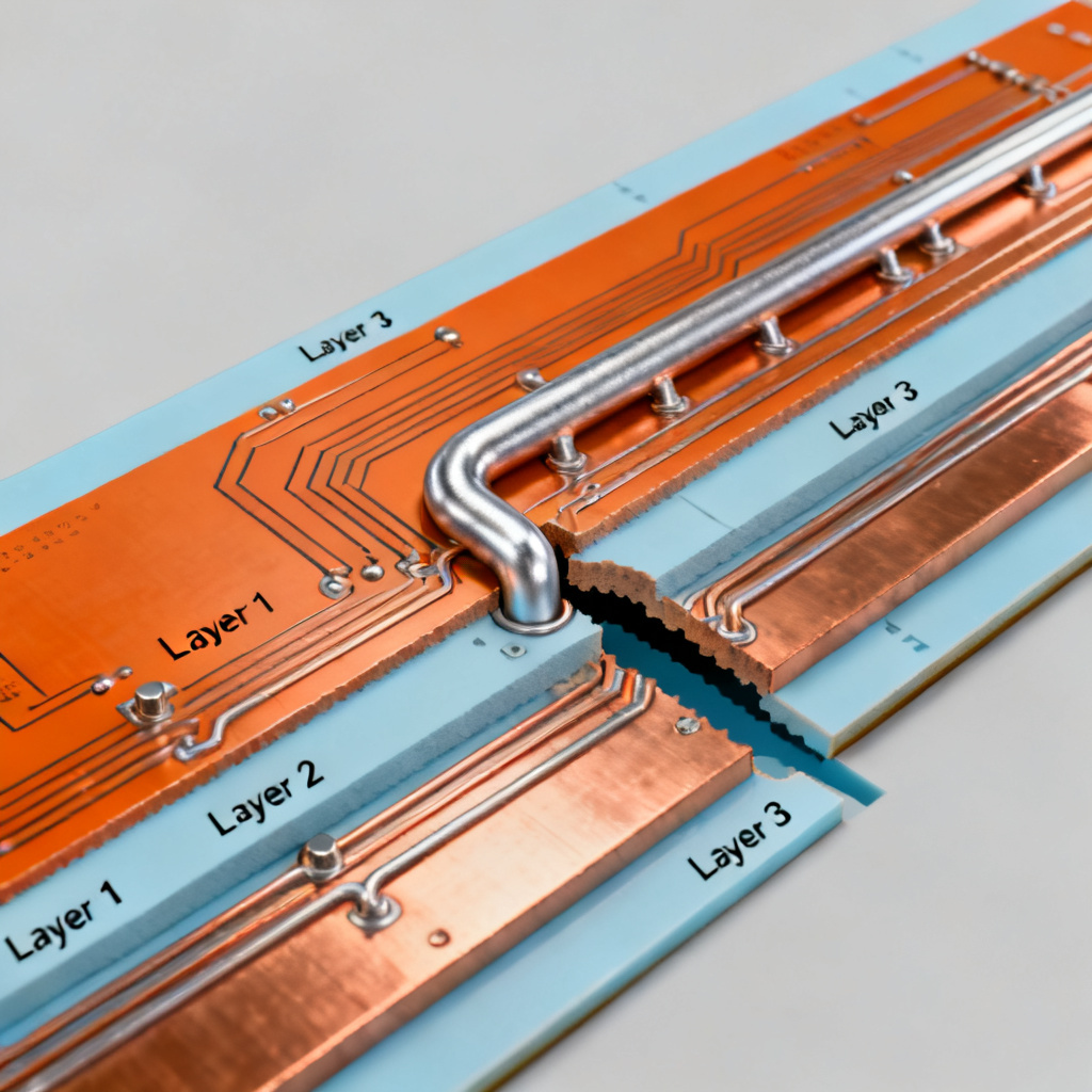
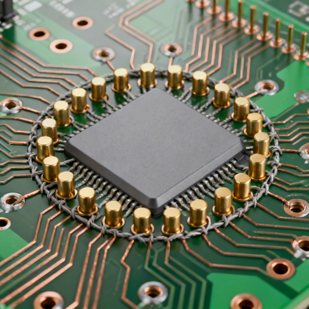
When a high-speed signal transitions layers through a via, the return path current must also switch reference planes. The via’s anti-pad creates a physical gap in the reference plane, forcing the return current to find an alternative path—often through parasitic capacitance or the via barrel itself. This increases loop inductance, causing signal reflections, ringing, and EMI. For example, a signal moving from Layer 1 (referenced to Ground Plane 1) to Layer 3 (referenced to Ground Plane 2) must jump planes; without a nearby ground via, the return path gap becomes a significant impedance discontinuity.
Specific Scenarios Where Gaps Occur
Layer transitions without a reference plane, multiple reference planes, and via stubs all exacerbate the return path gap. In designs with power and ground planes, a via may pass through several layers; if not properly stitched, the return current must travel through plane-to-plane capacitance, which is insufficient at high frequencies. Via stubs (unused barrel portions) also create resonant cavities that disrupt the return path.
Impact on Signal Integrity
The return path gap results in increased inductance, impedance discontinuity, EMI/EMC issues, and crosstalk. These effects degrade high-speed signal quality, causing overshoot, undershoot, and increased bit error rates in B2B PCB applications.
What to Do: Mitigation Techniques for Return Path Gap
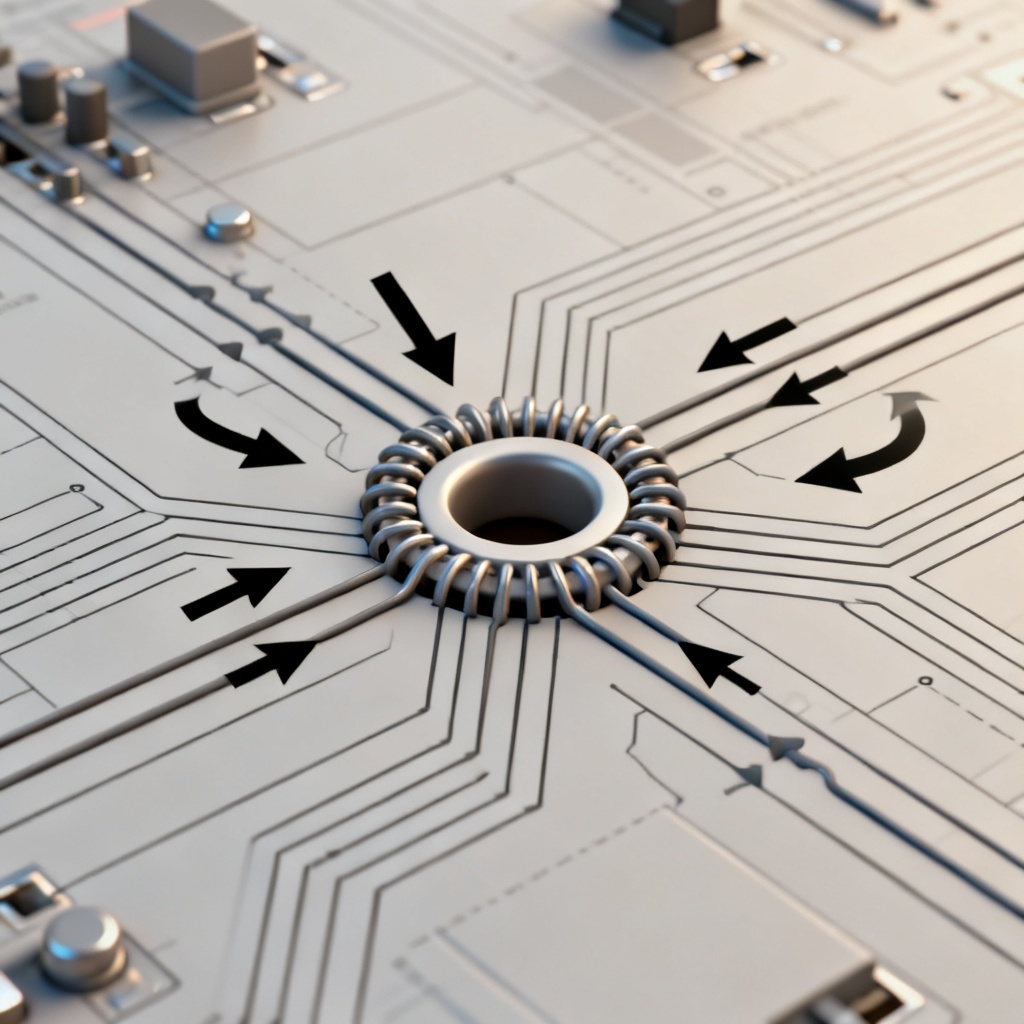
Use Grounding Vias (Stitching Vias)
Place a ground via (or multiple ground vias) as close as possible to the signal via—within 0.5 mm (20 mils). This provides a low-impedance return path, maintaining continuous current flow. For signals above 1 Gbps, use multiple ground vias to reduce inductance further.
Optimize Via Geometry
Reduce the anti-pad diameter to minimize the gap, but ensure adequate clearance. Use via-in-pad (VIP) with filled and capped vias for high-density designs. Back-drill via stubs to eliminate resonance, especially for signals above 10 Gbps.
Maintain Consistent Reference Planes
Always route high-speed signals adjacent to a solid ground plane. Avoid split planes; if unavoidable, use stitching capacitors to bridge the gap. Optimize layer stackup so signal layers are paired with ground layers.
Place Decoupling Capacitors
For power plane transitions, place low-ESL decoupling capacitors (e.g., 0.1 µF to 1 µF) near the via to provide a low-impedance return path at high frequencies.
Use Differential Vias for Differential Signals
For differential pairs, place ground vias symmetrically around the signal via pair to maintain return path symmetry and prevent common-mode noise.
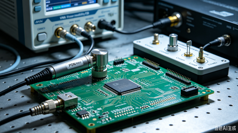
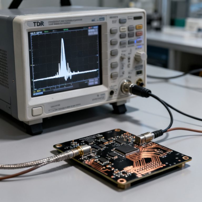
Simulate and Validate
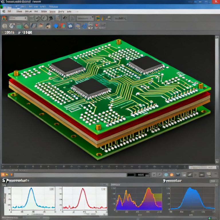
Use 3D EM simulation tools (e.g., Ansys HFSS, CST) to model via transitions and return path gaps. Validate with TDR to identify impedance discontinuities.
Practical Design Examples and Case Studies
Case Study 1: Single-Ended High-Speed Signal (10 Gbps)
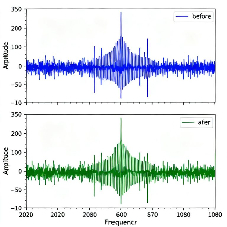
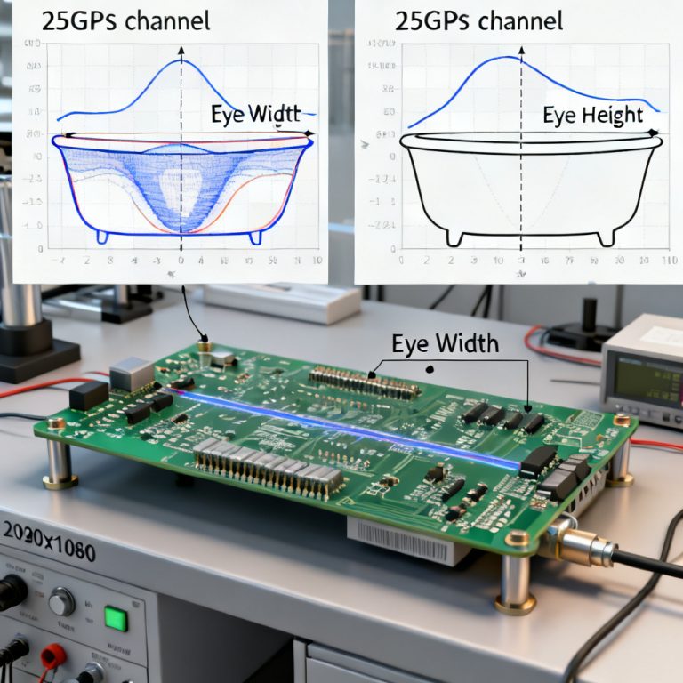
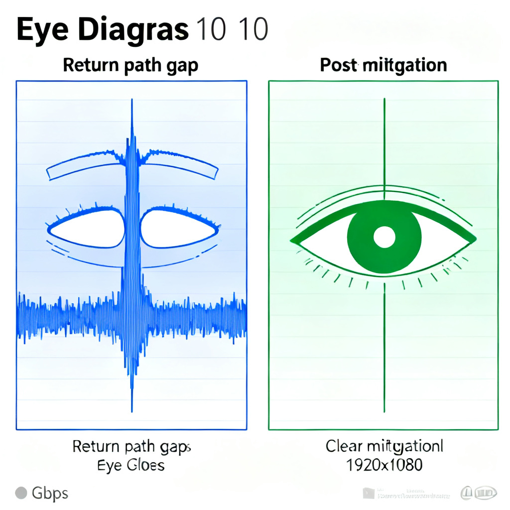
A 10 Gbps signal on a 4-layer board transitioning from Layer 1 to Layer 4 without a ground via showed a 15% impedance drop. Adding a ground via 0.3 mm away reduced the drop to 3%. Back-drilling eliminated stub resonance, improving the eye diagram.
Case Study 2: Differential Pair in a 16-Layer Board
A differential pair transitioning through multiple power planes caused common-mode noise. Placing ground vias next to each signal via and adding a 0.1 µF decoupling capacitor improved CMRR by 10 dB.
Case Study 3: High-Density Interconnect (HDI) Design
Microvias in HDI designs created small return path gaps. Using stacked microvias with via-in-pad and copper filling maintained signal integrity up to 28 Gbps.
B2B Manufacturing Considerations for Return Path Gap
| Parameter | Recommendation | Impact on Return Path Gap |
|---|---|---|
| Ground via distance from signal via | ≤ 0.5 mm | Reduces loop inductance |
| Anti-pad diameter | Minimize per DFM limits | Reduces physical gap |
| Back-drilling depth | Remove stubs > 0.5 mm | Eliminates resonance |
| Decoupling capacitor value | 0.1 µF – 1 µF | Bridges power plane transitions |
When working with a B2B PCB manufacturer, specify via types (through-hole, blind, buried, microvias), request back-drilling and via-in-pad, and review layer stackup for consistent reference planes. Balance cost vs. performance: for moderate speeds (up to 5 Gbps), simple ground vias may suffice.
Frequently Asked Questions about Via Return Path Gap
What is a return path gap in high-speed PCB design?
A return path gap occurs when a via transition disrupts the continuous low-impedance return path for a high-speed signal, typically caused by the anti-pad in the reference plane. This increases loop inductance and degrades signal integrity.
How do vias create a gap in the return path?
Vias create a gap because the anti-pad physically removes copper from the reference plane, forcing the return current to find an alternative path. Without a nearby ground via, this results in a large loop area and impedance discontinuity.
What is the best way to fix a return path gap in PCB design?
The best fix is to place a ground via (stitching via) as close as possible to the signal via—within 0.5 mm. For high-speed designs, use multiple ground vias, back-drilling, and optimize via geometry to minimize the gap.
Does via-in-pad help reduce return path gap?
Yes, via-in-pad with filled and capped vias eliminates the anti-pad gap entirely, providing a continuous return path. This is especially useful for high-density interconnect (HDI) designs.
How does back-drilling affect the return path?
Back-drilling removes unused via stubs, which can create resonant cavities that disrupt the return path. This improves signal integrity for high-speed signals above 10 Gbps.
Return path gap is a critical issue in high-speed PCB design. Grounding vias provide a low-impedance return path. Via geometry optimization minimizes discontinuities. Back-drilling eliminates stub resonance. Decoupling capacitors bridge power plane transitions. Simulation tools validate via performance.