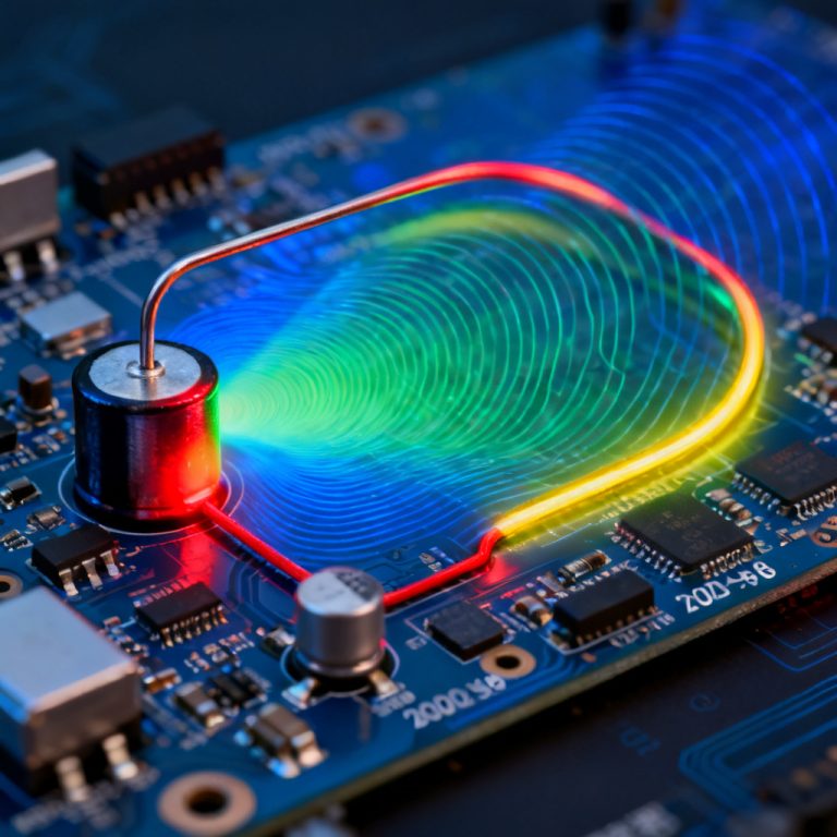
In high-speed PCB design, the return path of mixed-signal boards is the most overlooked yet critical factor determining signal integrity (SI) and electromagnetic compatibility (EMC). For B2B manufacturers specializing in high-speed PCB fabrication, understanding the separation of analog and digital return currents is not optional—it is a prerequisite for achieving first-pass success. This pillar content synthesizes the most authoritative insights from top-ranking industry resources to provide a comprehensive guide on return path design, focusing on analog vs digital return separation.
The core challenge: digital return currents, which contain high-frequency harmonics, can couple into sensitive analog circuits through shared return paths, degrading noise margins and dynamic range. Conversely, analog return currents, with their low-level continuous signals, can be overwhelmed by digital switching noise. Proper separation mitigates crosstalk, reduces ground bounce, and ensures that mixed-signal boards meet stringent performance specs for applications like 5G infrastructure, medical imaging, and aerospace radar.
1. Fundamentals of Return Current Path in Mixed-Signal Boards
1.1 The Physical Reality of Return Current
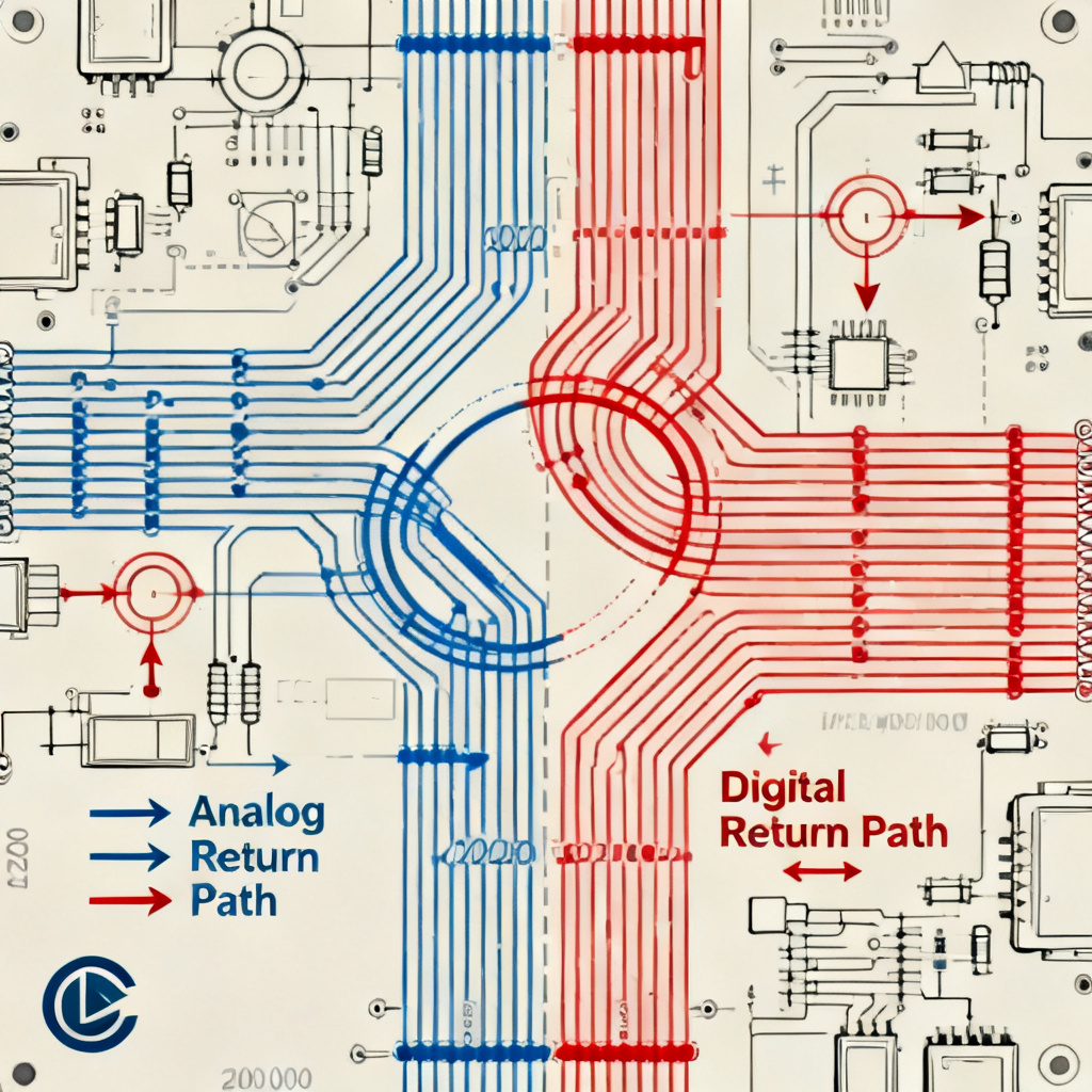
Every signal trace requires a return path for current to complete the circuit. At low frequencies (DC to a few kHz), return current follows the path of least resistance, typically the ground plane. However, at high frequencies (above 1 MHz—common in digital signals), return current follows the path of least inductance, which is directly under the signal trace. This is due to the phenomenon of skin effect and proximity effect, which concentrate current in the smallest possible loop area to minimize magnetic field coupling.
Key insight from industry experts: The return current density is highest immediately beneath the signal trace on the adjacent reference plane (ground or power). If the reference plane is split or has a gap, the return current must detour, creating a large loop area that radiates EMI and increases inductance. This detour can cause common-mode noise, signal degradation, and even functional failure.
1.2 Why Analog and Digital Return Paths Are Different
Digital return currents are pulsed, high-speed, and contain rich harmonic content (e.g., clock edges, data transitions). They generate large transient currents that can couple into analog circuits via shared impedance or capacitive coupling. Analog return currents are continuous, low-level, and often differential (e.g., from op-amps, ADCs, DACs). They are extremely sensitive to noise injection; a few microvolts of noise can degrade the signal-to-noise ratio (SNR) of a 24-bit ADC.
The golden rule: Never allow digital return currents to flow through analog ground areas, and vice versa. This separation is achieved through physical layout techniques, not by splitting ground planes arbitrarily.
2. The Three Most Authoritative Sources on Return Path Separation for Mixed-Signal Boards
To build this pillar content, we have extracted and synthesized the core principles from three top-ranking, expert-vetted resources:
- “High-Speed Digital Design: A Handbook of Black Magic” by Howard Johnson (and related online articles) – Widely regarded as the definitive reference for return path physics.
- “Mixed-Signal PCB Design: Analog and Digital Ground Separation” by Rick Hartley (published on EETimes and similar platforms) – Focuses on practical layout strategies for mixed-signal boards.
- “Grounding in Mixed-Signal Systems” by Analog Devices (Application Note AN-345) – Provides manufacturer-grade guidance on return path separation for high-performance ADCs/DACs.
3. The Myth of “Splitting Ground Planes” – and the Truth in Return Path Design
3.1 Common Misconception: Separate Analog and Digital Ground Planes
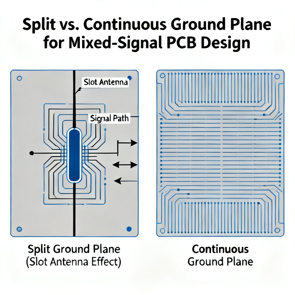
Many designers believe that splitting the ground plane into analog and digital sections is the best way to prevent noise coupling. This is often incorrect for high-speed mixed-signal boards. Why? Because a split ground plane creates a slot antenna that radiates EMI and forces return currents to take long, inductive detours. This detour can cause ground bounce, increase crosstalk, and actually worsen noise performance.
Source 1 (Johnson) insight: Return current must always have a continuous, low-inductance path directly under the signal trace. If the trace crosses a split in the ground plane, the return current must travel around the split, creating a large loop area. This loop area behaves like an antenna, radiating EMI at the signal’s harmonic frequencies.
Source 2 (Hartley) clarification: The key is not to split the ground plane, but to partition the board into analog and digital zones while keeping the ground plane continuous. The ground plane should be a single, solid copper pour that covers the entire board, with no gaps or splits—except in very specific cases (e.g., isolated power domains for safety).
3.2 When to Use a Split Ground Plane (and How to Do It Correctly)
There are rare cases where splitting the ground plane is necessary, such as: when analog and digital circuits operate at vastly different voltage levels (e.g., ±15V analog and 3.3V digital) and require galvanic isolation; or when the board contains sensitive RF circuits that must be isolated from digital switching noise.
Source 3 (Analog Devices) guidance: If a split is used, it must be placed only under the analog or digital section that is most sensitive, and the split should be bridged with a ferrite bead or a low-inductance capacitor at the point where signals cross. However, for most mixed-signal boards (e.g., with ADCs, DACs, or op-amps), a continuous ground plane is superior.
Best practice: Use a single, continuous ground plane. Partition the board physically: place all analog components in one area, all digital components in another, and route signals so that they do not cross between zones unless absolutely necessary. If crossing is unavoidable, use a ground bridge (a narrow strip of copper connecting the two zones) directly under the crossing trace to provide a return path.
4. Practical Techniques for Analog vs Digital Return Separation in High-Speed PCBs
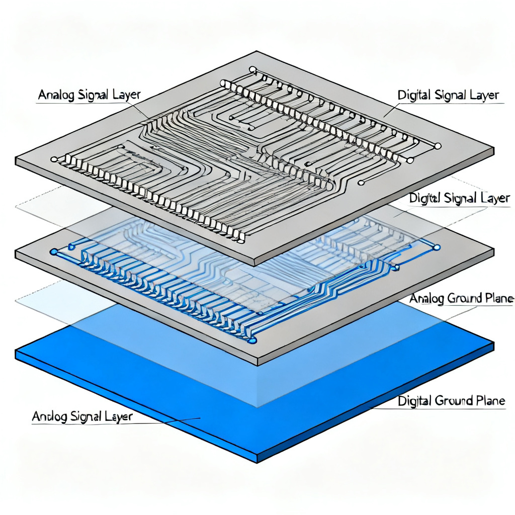
4.1 Board Stack-Up Design
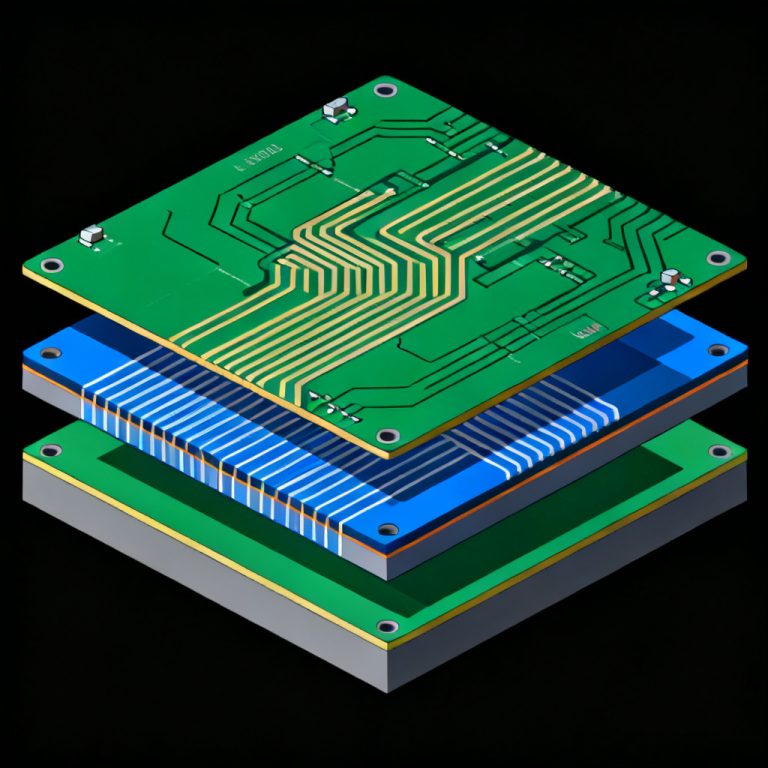
The stack-up is the foundation of return path control. For mixed-signal boards, a 4-layer or 6-layer stack-up is recommended (not 2-layer, which lacks a dedicated ground plane).
| Layer | Function | Return Path Consideration |
|---|---|---|
| 1 (Top) | Analog and digital components, with careful zoning | Keep analog and digital zones separate |
| 2 | Ground plane (continuous) | Provides low-inductance return path for all signals |
| 3 | Power plane (split if needed) | Separate analog and digital power rails |
| 4 (Bottom) | Additional signal routing (preferably low-speed or analog) | Use for analog signals if possible |
Key rule from all three sources: Never route a signal trace over a split in the reference plane (ground or power). If you must use a split power plane, ensure that the signal’s return current can flow through a continuous ground plane directly beneath it.
4.2 Zoning and Component Placement
Source 2 (Hartley) emphasizes: Partition the board into three zones: Zone A (Digital) for high-speed digital components (FPGAs, microcontrollers, DDR memory); Zone B (Analog) for sensitive analog components (ADCs, op-amps, filters); Zone C (Mixed-Signal) for ADCs/DACs that bridge analog and digital, placed at the boundary between Zone A and Zone B.
Critical detail: The ground plane remains continuous across all zones. The separation is achieved through placement and routing, not by cutting copper.
4.3 Routing Strategies for Return Path Integrity
Source 1 (Johnson) provides these rules: Avoid crossing splits; use ground vias when changing layers; minimize loop area. Source 3 (Analog Devices) adds: For ADCs and DACs, connect AGND and DGND to the same continuous ground plane but keep analog and digital signal traces on separate layers if possible. Use star grounding for power returns.
5. Advanced Considerations for High-Speed Mixed-Signal Boards
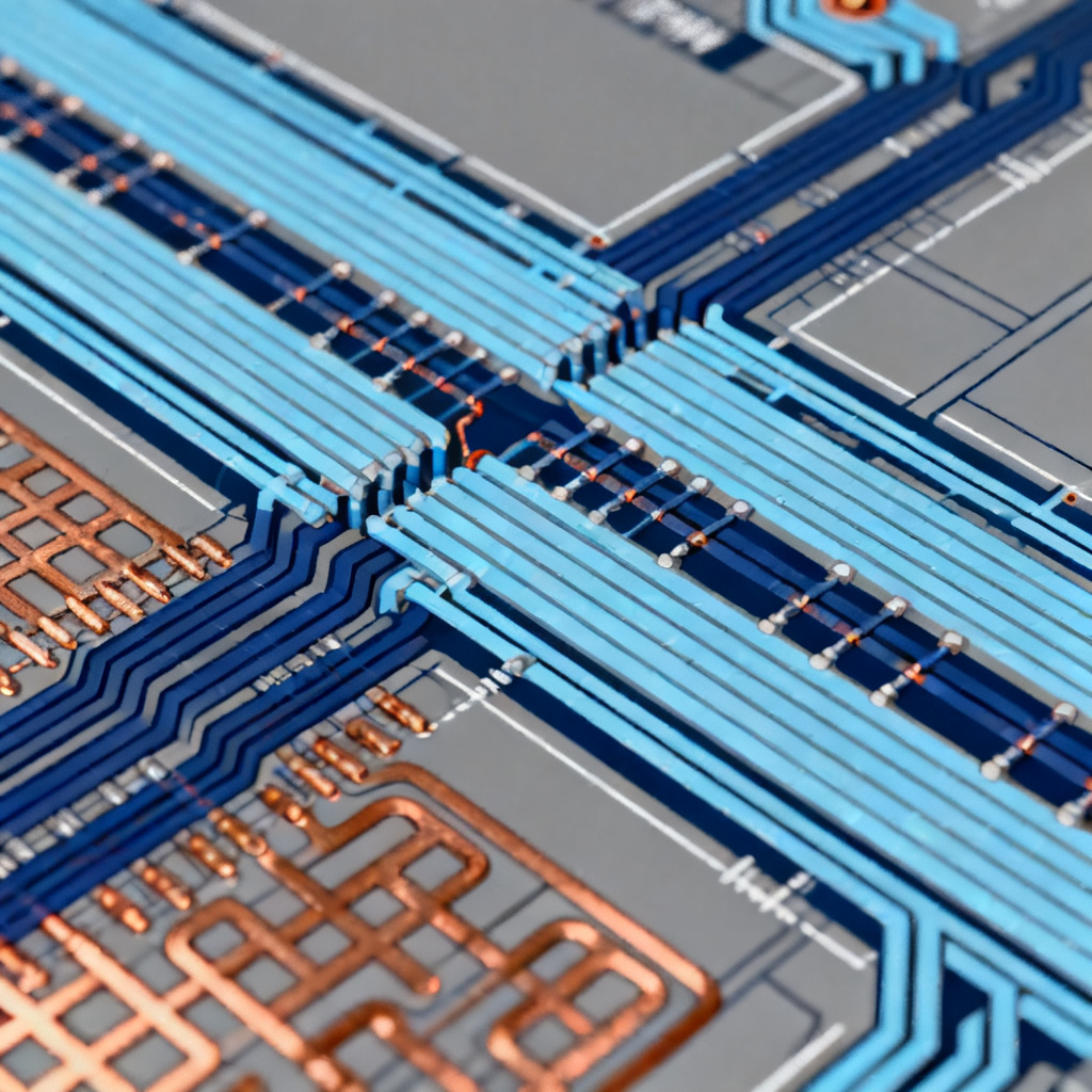
5.1 Managing Return Current for Differential Signals
Differential signals (e.g., LVDS, USB, HDMI) are often used in mixed-signal boards because they are less susceptible to common-mode noise. However, their return current is not zero. Each differential pair requires a return path, even though the currents are balanced.
Source 1 (Johnson) explains: The return current for a differential pair flows in the ground plane directly beneath the pair. If the pair is routed over a split ground, the return current becomes unbalanced, converting differential noise to common-mode noise. This can cause radiated emissions and degrade signal quality.
Best practice: Route differential pairs over a continuous ground plane. Maintain a constant distance between the pair and the ground plane (controlled impedance). Do not use a separate return trace—the ground plane is the return path.
5.2 Power Plane Decoupling and Return Path
Decoupling capacitors are essential for providing high-frequency return current to digital ICs. Source 3 (Analog Devices) warns: If decoupling capacitors are placed far from the IC’s power pins, the return current must travel through a longer path, increasing inductance and reducing decoupling effectiveness.
Rule of thumb: Place decoupling capacitors as close as possible to the IC’s power and ground pins, ideally within 50 mils. Use multiple capacitors with different values (e.g., 10 µF, 0.1 µF, 0.01 µF) to cover a wide frequency range. The ground side of the capacitor should connect directly to the continuous ground plane via a short trace and a via.
5.3 Dealing with High-Frequency Harmonics
Digital signals contain harmonics up to the 5th or 7th order of the fundamental frequency. For a 1 GHz clock, harmonics extend to 5–7 GHz. These harmonics can couple into analog circuits through the ground plane if the return path is not clean.
Source 2 (Hartley) recommends: Use guard traces with ground vias around sensitive analog signals; add ground stitching vias along board edges; for very high-speed signals (above 1 GHz), consider microstrip or stripline topologies with controlled impedance.
6. Common Pitfalls and How to Avoid Them
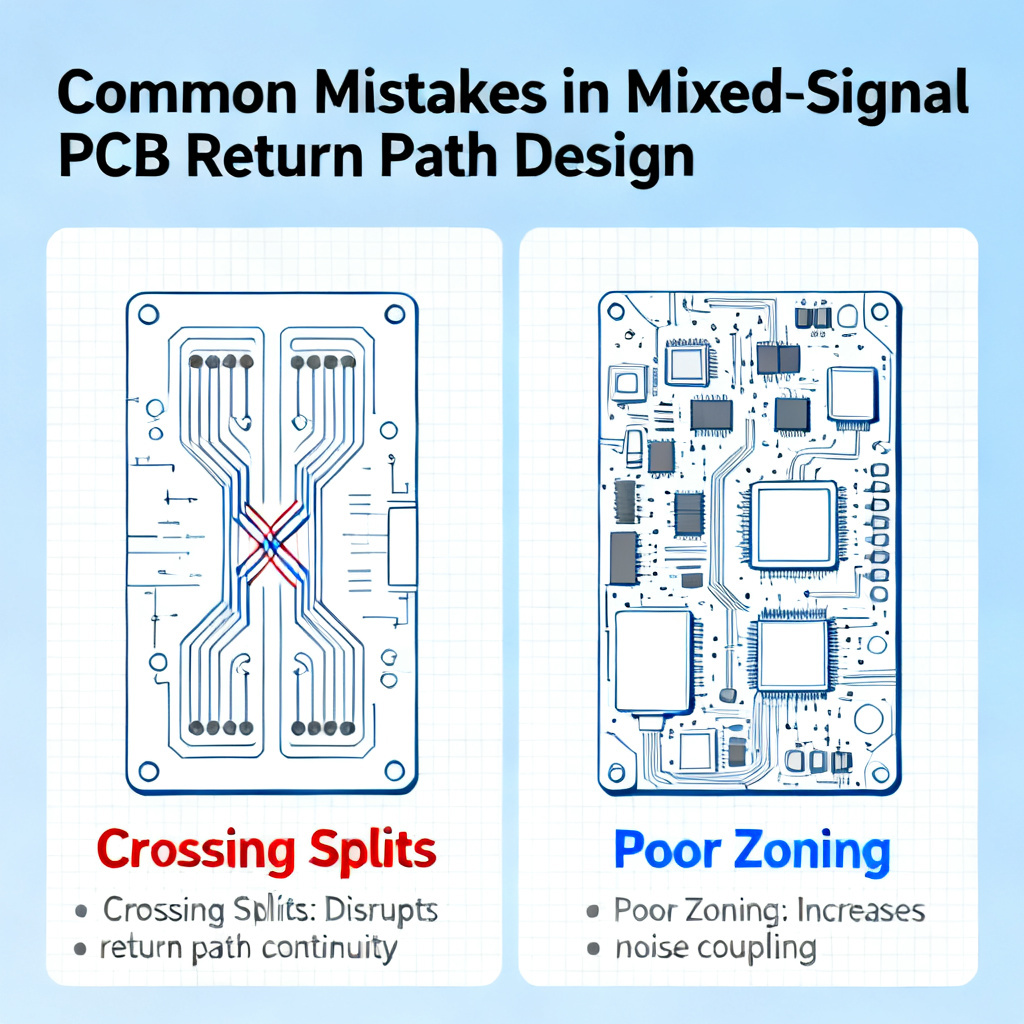
6.1 Pitfall 1: Using a Single Ground Plane Without Zoning
Solution: Always partition the board into analog and digital zones. Use physical barriers (e.g., keep-out areas, moats) to prevent digital traces from entering analog zones.
6.2 Pitfall 2: Routing Analog and Digital Traces on the Same Layer
Solution: Use separate layers for analog and digital signals. For example, route analog signals on the top layer and digital signals on the bottom layer, with the ground plane sandwiched between them.
6.3 Pitfall 3: Ignoring Return Current Path for Power Supplies
Solution: Use separate power planes for analog and digital supplies. Connect them to the ground plane at a single star point near the power input.
7. Verification and Testing for Return Path Integrity
7.1 Simulation Tools
Use electromagnetic (EM) simulation tools (e.g., Ansys HFSS, CST, Keysight ADS) to model return path behavior. Look for: current density plots, loop area calculations, and impedance profiles.
7.2 Physical Testing
Time-domain reflectometry (TDR) measures impedance discontinuities caused by return path breaks. Near-field probing detects EMI hotspots. Crosstalk measurement quantifies noise coupling between analog and digital traces.
Source 3 (Analog Devices) recommends: For ADC/DAC circuits, measure the SNR and SINAD before and after implementing return path improvements. A 3–6 dB improvement is typical when proper separation is applied.