Master DDR5 PCB design with a deep dive into the Return Path PCB Design for DDR5: Data Strobe Reference Plane Requirements. Learn about return path discontinuity, via optimization, and stack-up strategies for reliable high-speed signal integrity in your next PCB project.
The Criticality of the Return Path in DDR5
The transition from DDR4 to DDR5 memory has brought a paradigm shift in signal integrity (SI) requirements. Operating at data rates exceeding 6.4 Gbps, the margin for error in DDR5 PCB design is virtually zero. While the industry often focuses on the differential Data (DQ) and Data Strobe (DQS) pairs, the unsung hero of a successful layout is the return path—the silent, continuous reference plane that allows these high-speed signals to propagate cleanly.
This pillar page synthesizes the most authoritative expert knowledge on the subject. We will dissect the specific requirements for the DDR5 Data Strobe (DQS) reference plane, focusing on the physics of the return current, the pitfalls of via transitions, and the absolute necessity of a low-inductance path. This is not just a theoretical exercise; it is the practical blueprint for achieving first-pass success in your DDR5 PCB designs.
The Physics of the Return Path: Why DQS Demands More
To understand the DQS reference plane requirements, we must first revisit the fundamental physics of signal propagation. A high-speed signal is not a single-ended entity traveling down a trace; it is a transverse electromagnetic (TEM) wave that propagates between the signal trace and its adjacent reference plane.
The Principle of Least Inductance
The return current for a high-speed signal does not take the path of least resistance (DC). Instead, it takes the path of least inductance. This path is directly under the signal trace, on the adjacent reference plane. For a differential pair like the DQS (DQS_t and DQS_c), the return current flows in the plane directly beneath the pair, mirroring the signal’s path.
Why DDR5 DQS is More Sensitive
- Higher Frequencies: DDR5’s doubled data rate compared to DDR4 means the fundamental and harmonic frequencies of the DQS signal are significantly higher. At these frequencies, even a small inductance (a few nanohenries) from a poor return path creates a large impedance discontinuity.
- Strict Jitter and Timing Budgets: The DQS signal is the clock for the DQ bus. Any jitter or skew introduced onto the DQS directly translates to timing errors on all data bits. A compromised return path for DQS creates common-mode noise and mode conversion, degrading the signal’s eye diagram.
The Reference Plane as a Waveguide
The reference plane (typically a ground plane, VSS) acts as a waveguide. A continuous, unbroken plane ensures that the return current can flow unimpeded. Any break, slot, or change in the plane’s geometry forces the return current to detour, increasing the loop inductance. This inductance manifests as:
- Increased Signal Attenuation: Energy is lost to radiated emissions and ground bounce.
- Impedance Discontinuity: The instantaneous impedance of the trace changes over the break, causing reflections.
- Common-Mode Noise: The differential signal’s electromagnetic field becomes unbalanced, converting some of the differential energy into common-mode noise, which is highly susceptible to radiation and crosstalk.
The Data Strobe (DQS) Reference Plane: Ground (VSS) vs. Power (VDDQ)
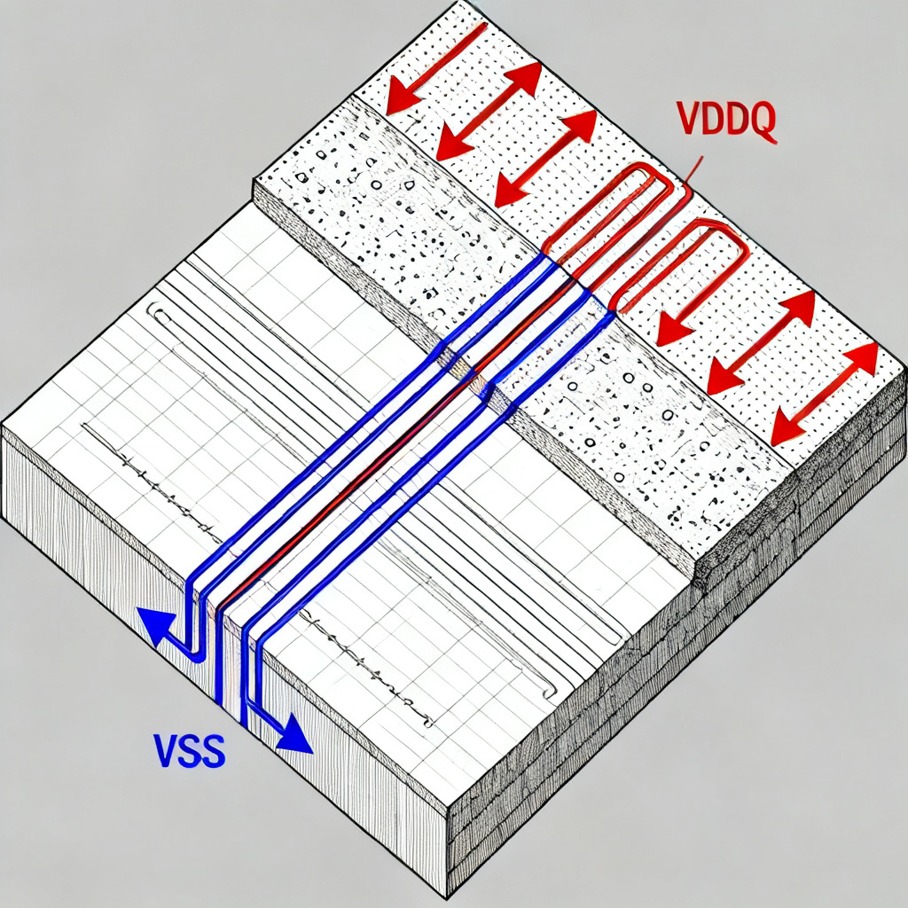
One of the most critical decisions in DDR5 layout is the assignment of the reference plane for the DQS differential pair. The industry’s top experts are unanimous on this point.
The Expert Consensus: The DQS must be referenced to a solid, continuous Ground (VSS) plane.
Why VSS over VDDQ?
- Stability and Noise: A VSS (ground) plane is the most stable, lowest-noise reference in the entire system. It is the universal return path for all signals. A VDDQ (power) plane, while also a DC reference, carries switching noise from the memory controller and DRAM’s I/O buffers. This noise couples directly onto the DQS signal if it is used as the reference.
- Return Path Integrity at Via Transitions: This is the most compelling reason. When a DQS signal transitions from one layer to another via a via, the return current must also change reference planes. If the signal is referenced to VSS on both layers, the return current can easily transfer through a stitching via connected to the VSS plane. If the signal is referenced to VDDQ on one layer and VSS on another, the return current must find a path through a decoupling capacitor (a high-impedance path at high frequencies), creating a massive discontinuity.
- Simplified Stack-up: A standard 8-layer or 10-layer stack-up for DDR5 typically dedicates multiple layers to VSS. Using VSS as the primary reference for all critical signals (DQS, DQ, Address/Command) simplifies the design and ensures a consistent, low-impedance return path.
The Exception (and its strict rules)
Some high-density designs may force a DQS pair to be referenced to VDDQ for a short, unavoidable segment. If this is necessary, it is mandatory to place a high-density array of 0402 or 0201 decoupling capacitors (typically 100nF) directly adjacent to the via transition point. This provides a low-inductance AC path for the return current to jump from VDDQ to VSS. However, this is a last-resort technique and should be avoided if at all possible.
The Via Transition: The Most Common Return Path Killer
The transition of a DQS signal through a via is the single most critical point for return path integrity. The signal’s path is simply the via barrel. The return current’s path is far more complex.
The Problem
When a DQS pair switches from a top-layer trace (referenced to Layer 2 VSS) to a bottom-layer trace (referenced to Layer N-1 VSS), the return current must also move from Layer 2 to Layer N-1. If there is no dedicated, low-inductance path for this current, it will find the path of least inductance, which is often through the nearest VSS via—which could be far away.
The Solution: The “Stitching Via” or “Return Via”
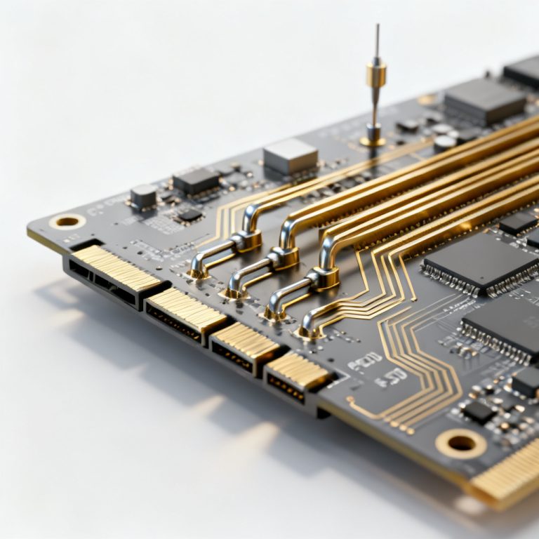
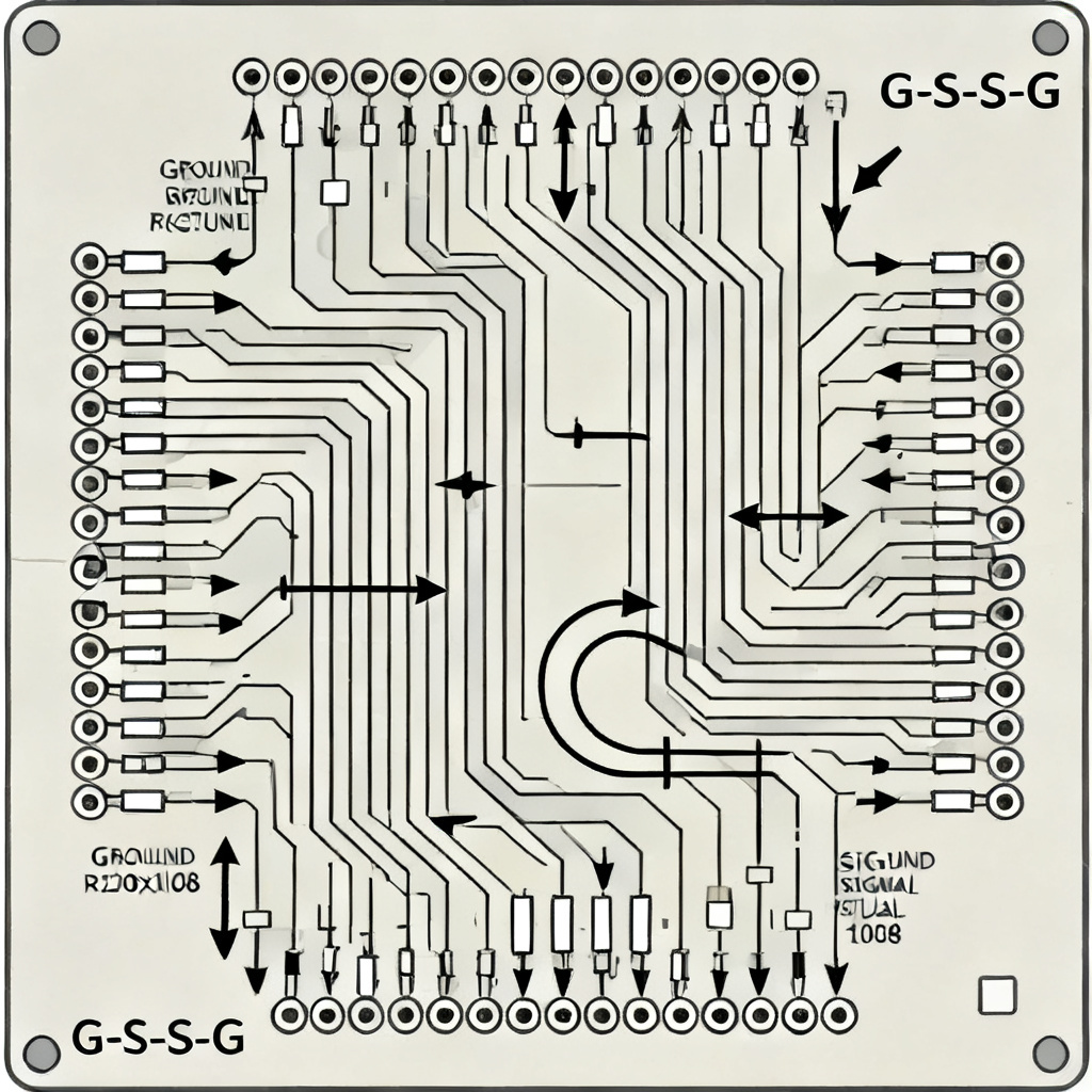
To solve this, the expert community mandates the use of ground stitching vias. These are VSS vias placed in very close proximity to the signal vias.
Optimal Via Configuration for a DQS Differential Pair
- The “G-S-S-G” Pattern: For a single-ended trace, the ideal is a signal via with a ground via adjacent to it. For a differential pair, the most robust configuration is to place a ground via on either side of the signal via pair. The pattern, looking from above, is: GND (VSS) – DQS_t – DQS_c – GND (VSS).
- Spacing: The distance between the center of the signal via and the center of the ground via should be as small as possible. A general rule of thumb is less than 40 mils (1mm). The ideal is to use the smallest pitch via pad size possible and place them as close as the design rules allow.
- Via-in-Pad (VIP) for Ground: For the ultimate in performance, consider using Via-in-Pad (VIP) technology for the ground stitching vias. This eliminates the short stub of the via pad and allows the via to be placed directly in the plane, minimizing loop inductance. This is a premium technique that high-speed PCB manufacturers (like our facility) specialize in.
- Anti-Pad Management: The anti-pad (the clearance hole around the via on the reference plane) must be carefully managed. An oversized anti-pad on the VSS plane increases the loop area. The anti-pad should be just large enough to provide the required clearance for the via barrel, without unnecessarily removing copper from the return path.
Visualizing the Current Flow
Imagine the return current as a rubber band. Under the trace, it is stretched taut directly underneath. When it hits the via, it must snap around the via’s anti-pad and then jump to the nearest ground via. The closer the ground via, the shorter the “snap,” and the lower the inductance.
Stack-Up Strategies for DDR5 DQS
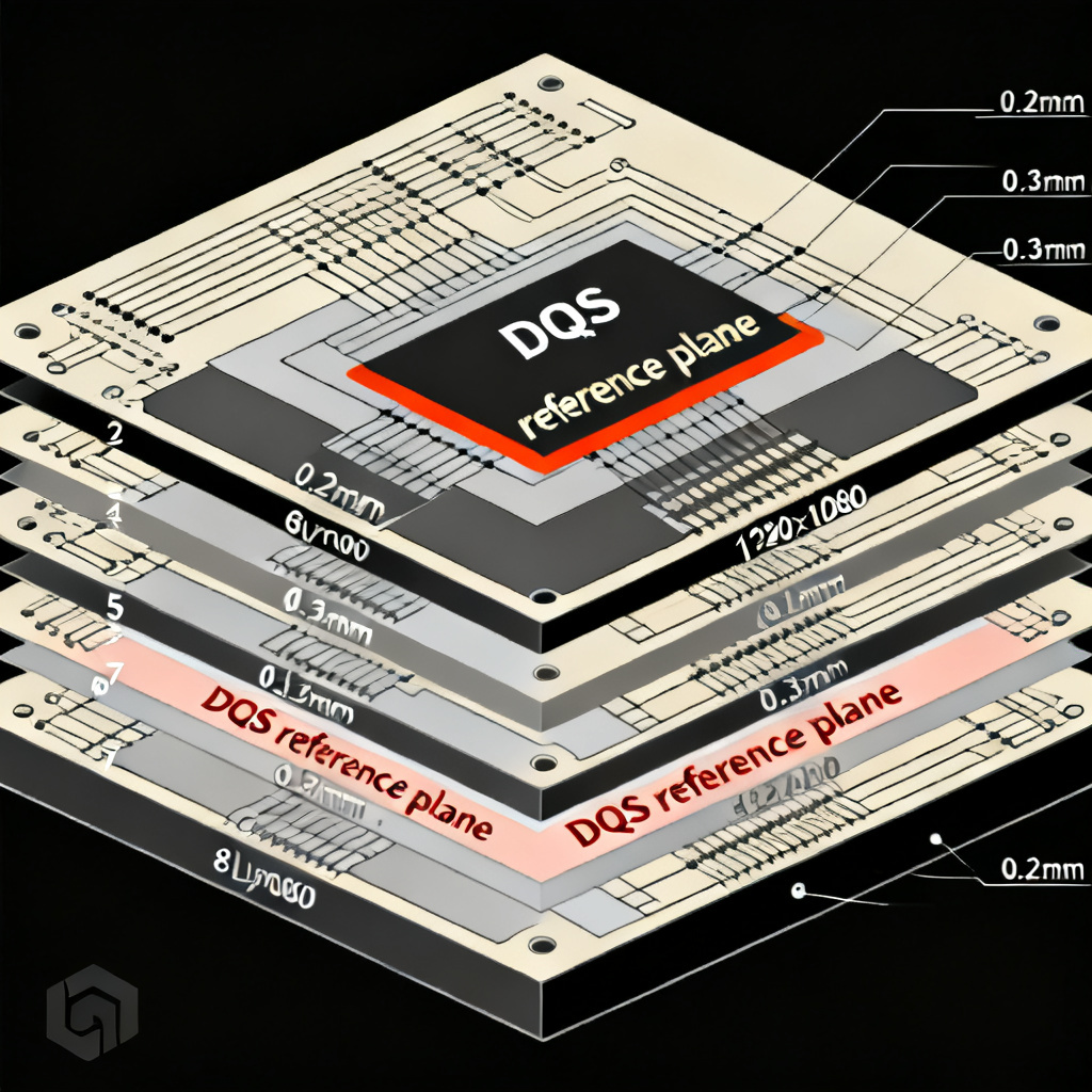
The PCB stack-up is the foundation upon which all return path integrity is built. The primary goal is to create a tightly coupled transmission line environment.
| Layer | Signal/Plane | Notes |
|---|---|---|
| Layer 1 | Top | DQS, DQ, Critical High-Speed Traces |
| Layer 2 | Ground (VSS) | Continuous, unbroken plane. The primary reference for Layer 1. |
| Layer 3 | Signal (Lower Speed) | Address/Command, Control |
| Layer 4 | Ground (VSS) | Continuous plane. Important for Layer 3 and 5 return. |
| Layer 5 | Power (VDDQ, VDD) | Split as needed. |
| Layer 6 | Ground (VSS) | Continuous plane. Important for Layer 7 return. |
| Layer 7 | Signal | DQS, DQ (if needed), other High-Speed Traces |
| Layer 8 | Ground (VSS) | Continuous, unbroken plane. The primary reference for Layer 7. |
Key Principles
- Adjacent Ground Planes: Every high-speed signal layer (specifically the layers carrying DQS) must be directly adjacent to a solid, continuous VSS plane. This is non-negotiable. A 2-layer or 4-layer board is fundamentally unsuitable for reliable DDR5 routing.
- Tight Dielectric: The distance between the signal layer and its adjacent VSS plane (the pre-preg thickness) should be minimized. A thinner dielectric (e.g., 3.5 mils to 4 mils) creates a stronger coupling between the signal and its return path, reducing the loop inductance and allowing for narrower trace widths to achieve a target impedance (typically 40-50 ohms differential for DQS).
- No Plane Splits Under DQS: This is the cardinal rule. Never, under any circumstances, route a DQS differential pair over a split in its reference plane. A split creates a massive loop area and an unacceptable impedance discontinuity. If you must route over a split for a power plane (e.g., VDDQ), ensure the immediately adjacent reference plane (e.g., Layer 2 VSS) is completely solid and unbroken.
Routing and Clearance Rules for DQS
Beyond the reference plane, the physical geometry of the DQS trace itself must be meticulously controlled.
- Differential Impedance: Maintain a consistent differential impedance of 40-50 ohms (typically 40 ohms for DDR5, but check your controller/DRAM specs). This is achieved by controlling the trace width (W), trace spacing (S), and the dielectric height (H) to the reference plane. The goal is a tight coupling (small S) relative to the plane height.
- Length Matching: The intra-pair skew (length difference between DQS_t and DQS_c) must be minimized. The industry standard is to keep it under 1 ps (roughly 6-8 mils in FR4). The inter-pair skew (length difference between DQS and its associated DQ group) must also be tightly matched, typically within a few picoseconds.
- Clearance to Other Signals: DQS pairs must be isolated from other high-speed signals (especially Address/Command) and from other DQ groups. A common rule is a 3W or 5W spacing (3 to 5 times the trace width) from the center of the DQS pair to the center of the nearest aggressor trace. This prevents crosstalk.
- Avoid 90-Degree Bends: Use 45-degree chamfered bends or curved traces. 90-degree bends create a localized impedance change and can act as a source of radiation.
Manufacturing Considerations for Your DDR5 PCB
As a B2B manufacturer specializing in High-Speed PCBs, we understand that theoretical design is only half the battle. The manufacturing process must faithfully reproduce the designer’s intent.
- Controlled Impedance Tolerances: We guarantee impedance control to ±5% for your DQS lines. This requires precise control of the etching process, pre-preg material selection, and lamination pressure.
- Via Fill and Planarization: For via-in-pad on ground stitching vias, we use a conductive or non-conductive fill process that is then planarized. This ensures a flat surface for component soldering and eliminates the risk of voids in the via.
- Material Selection: For DDR5, standard FR4 is insufficient. We recommend high-speed laminates like Isola 370HR, Megtron 4/6, or equivalent, which have a lower and more stable dielectric constant (Dk) and dissipation factor (Df) at high frequencies.
- Back-Drilling: For through-hole vias that have long, unused stubs, we offer back-drilling. A long via stub acts as a resonant cavity that can severely degrade the DQS signal at DDR5 frequencies. Back-drilling removes this stub, significantly improving signal quality. This is a highly recommended option for any DDR5 design.
Conclusion: The Path to a Successful DDR5 Design
The design of a DDR5 PCB is a complex, multi-variable challenge. The Data Strobe (DQS) signal, with its demanding timing and noise requirements, is the ultimate test of your layout skills. By focusing on the return path—selecting a solid VSS reference plane, optimizing via transitions with ground stitching vias, employing a proper stack-up, and using precise routing rules—you can build a robust foundation for your design.
Remember, every nanohenry of inductance you eliminate from the return path translates directly to a wider eye-opening, lower jitter, and a more reliable product. When you are ready to manufacture your high-speed, high-reliability PCB, partner with a manufacturer who understands these nuances. Contact our engineering team to discuss your specific DDR5 stack-up and via requirements. We are here to turn your design into a high-performance reality.
Frequently Asked Questions
What is the return path in DDR5 PCB design?
The return path in Return Path PCB Design for DDR5: Data Strobe Reference Plane Requirements is the continuous reference plane (typically ground) that carries the return current for high-speed signals like the Data Strobe (DQS). A proper return path ensures signal integrity by minimizing loop inductance and impedance discontinuities.
Why is the DQS reference plane critical for DDR5?
The DQS reference plane is critical because the Data Strobe signal acts as the clock for the DQ bus. Any noise or discontinuity in the return path for the DQS reference plane introduces jitter and common-mode noise, directly impacting data timing and reliability in high-speed DDR5 designs.
How do I optimize via transitions for DDR5 DQS?
To optimize via transitions for DDR5 DQS, use ground stitching vias in a G-S-S-G pattern close to the signal vias. This provides a low-inductance return path for the DQS reference plane, reducing impedance discontinuity and improving signal integrity.
What stack-up is recommended for DDR5 DQS routing?
A recommended stack-up for DDR5 DQS routing includes dedicated ground planes adjacent to signal layers, such as an 8-layer board with Layer 2 and Layer 8 as solid VSS planes. This ensures a continuous return path for the DQS reference plane and maintains controlled impedance.
Can I use VDDQ as a reference plane for DQS?
While VDDQ can be used as a reference plane for DQS in dense designs, it is not recommended due to noise coupling. If unavoidable, place decoupling capacitors near via transitions to maintain a low-inductance return path for the DQS reference plane, but ground (VSS) is always preferred.