Mastering ripple and noise reduction techniques in power integrity PCB design is essential for high-speed digital and RF systems where supply voltages shrink below 1V and signal frequencies climb into the GHz range. This pillar content synthesizes proven strategies from industry-leading sources to help you achieve clean, stable power delivery.
Sources of Power Supply Ripple and Noise in Power Integrity PCB Design
Before implementing mitigation, diagnosing origins is critical. Ripple and noise reduction techniques in power integrity PCB design distinguish between ripple (periodic, low-frequency AC from switching converters) and noise (high-frequency, non-periodic disturbances from fast edge rates, parasitic elements, load transients, and crosstalk).
Key Sources
- Switching Regulator Ripple: Fundamental switching frequency and harmonics from buck, boost, or flyback converters.
- High-Frequency Noise: Caused by fast dV/dt and di/dt in digital ICs, leading to ground bounce and simultaneous switching noise (SSN).
- Parasitic Elements: PCB trace inductance, via inductance, and capacitor equivalent series inductance (ESL) create resonance circuits that amplify noise.
- Load Transients: Sudden current demand changes induce voltage droop or overshoot.
- Crosstalk from Signal Traces: High-speed signals couple EMI onto adjacent power planes.
Decoupling and Bypass Capacitor Networks for Ripple and Noise Reduction
The most fundamental strategy for ripple and noise reduction techniques in power integrity PCB design is a well-designed decoupling capacitor network providing a low-impedance path to ground for AC noise.
Capacitor Selection and Parasitics
Every capacitor has ESR and ESL. Above the self-resonant frequency (SRF), the capacitor becomes inductive. Select capacitors with an SRF well above the noise frequency of interest. For high-speed designs, use small-case sizes (0402 or 0201) with low ESL and low ESR (X7R or NP0/C0G dielectrics for stability).
Multi-Value Capacitor Arrays
Parallel multiple values (10 µF, 1 µF, 0.1 µF, 0.01 µF, 1 nF) but avoid anti-resonance peaks by using a spread of overlapping frequency responses or a single low-ESL 100 nF X7R in 0402 for broadband decoupling, supplemented by bulk electrolytic capacitors for low-frequency ripple.
Bulk Capacitors for Low-Frequency Ripple
For ripple below 1 MHz, bulk capacitors (10 µF to 1000 µF) store energy and smooth voltage ripple. Place them close to the regulator output but not necessarily at the IC power pin.
High-Frequency Bypass Capacitors
For noise above 10 MHz, use small-value capacitors (1 nF to 100 nF) with very low ESL. Place them as close as physically possible to the power pins of each active IC. Mount on the same layer or use micro-vias directly under BGA pads.
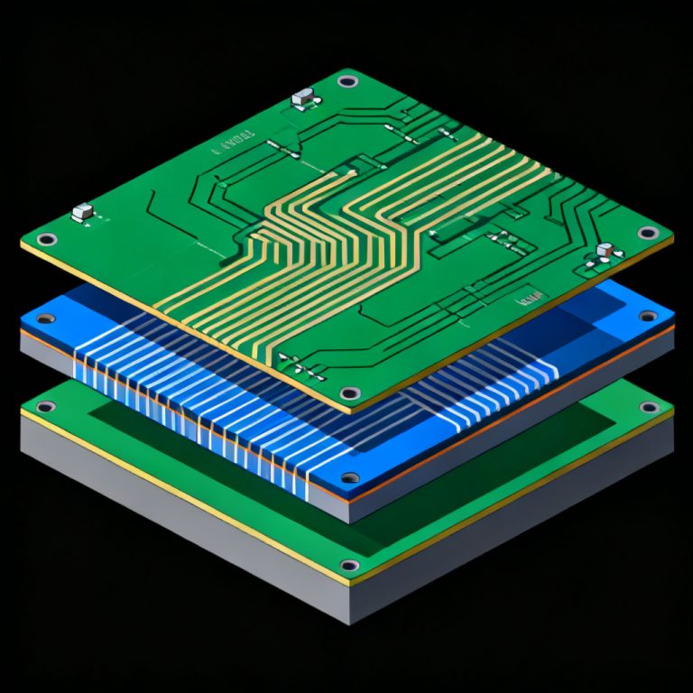
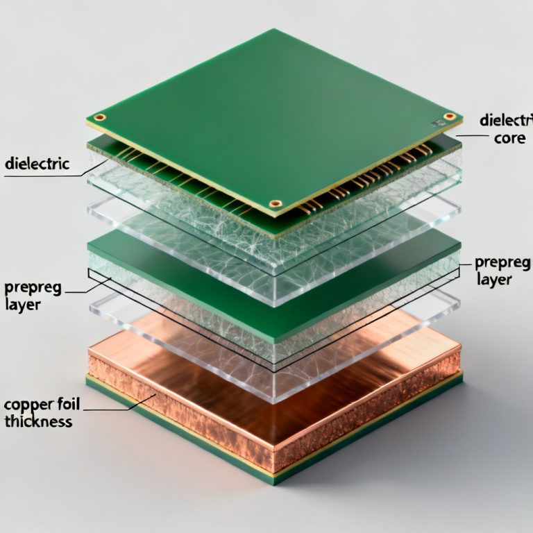
Advanced PCB Stackup and Layout Techniques for Power Integrity
Capacitor effectiveness depends entirely on PCB layout and stackup. Ripple and noise reduction techniques in power integrity PCB design must minimize loop inductance through dedicated, contiguous power and ground planes with thin dielectric (2–4 mils) to create a low-inductance parallel-plate capacitor.
Multiple Ground Planes and Via Stitching
Use multiple ground planes stitched with vias at every critical point—near IC power pins, connectors, and board edges—to prevent ground loops and ensure low-impedance return paths. Place a ground via within 1 mm of every power via.
Isolation of Sensitive Power Rails
For mixed-signal designs, physically separate analog and digital power planes with a slot or moat, but keep a single solid ground plane. Use ferrite beads in series with the power rail to isolate high-frequency noise, selecting beads with high impedance at the noise frequency and low DCR.
PDN Impedance Target
Calculate target impedance: Z_target = (V_rail × ripple_tolerance) / I_transient. For a 1.0V rail with 3% ripple and 5A transient, Z_target = 6 mΩ. The entire PDN must maintain impedance below this target across all frequencies. Use simulation tools (Ansys SIwave, Cadence Sigrity) to verify.
Optimized Via Placement and Anti-Pad Design
- Use multiple vias in parallel for each power/ground connection.
- Minimize via stub length with blind/buried vias or back-drilling.
- Reduce anti-pad clearance to the smallest reliable value (e.g., 10 mils) to lower via inductance.
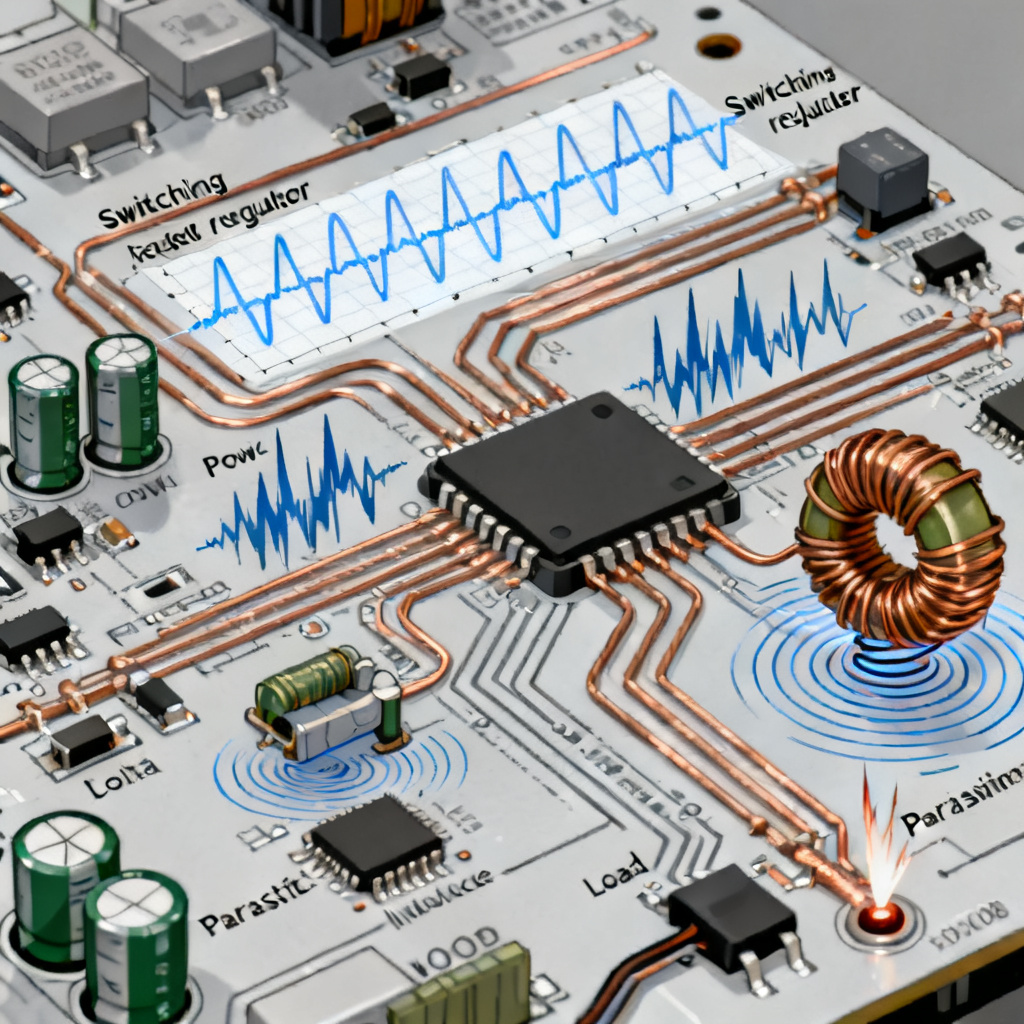
Filtering and Regulation Techniques for Ripple and Noise Reduction
Beyond capacitors and layout, active and passive filtering targets specific noise frequencies. Ripple and noise reduction techniques in power integrity PCB design include LC filters, π-filters, LDOs, ferrite beads, and common mode chokes.
LC and π-Filtering
For noisy rails (e.g., PLL supply), use an LC filter (inductor + capacitor) or π-filter (capacitor-inductor-capacitor). Choose an inductor with high SRF and low DCR. Cutoff frequency should be well below the noise frequency (e.g., 1/10th of switching frequency).
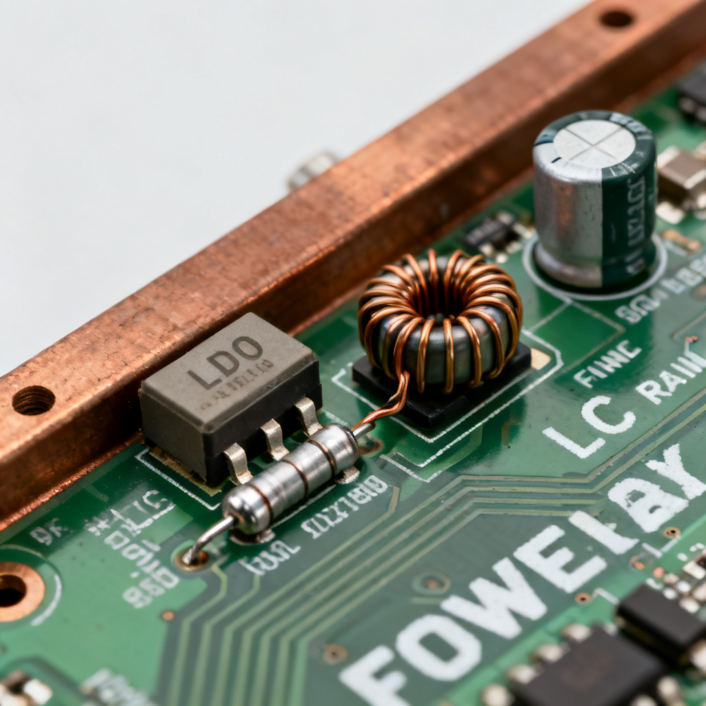
Low Dropout Regulators (LDOs)
An LDO provides ultra-low noise output with excellent PSRR. Place an LDO after a switching regulator to clean the rail. Pair with a low-ESL output capacitor. LDOs are ideal for noise-sensitive analog or RF subsections despite lower efficiency for high-current rails.
Ferrite Beads and Common Mode Chokes
Ferrite beads dissipate high-frequency noise as heat. Use on power input lines or individual IC power pins, but avoid on high-current rails where saturation may occur. Common mode chokes suppress in-phase noise on differential power lines, reducing radiated EMI.
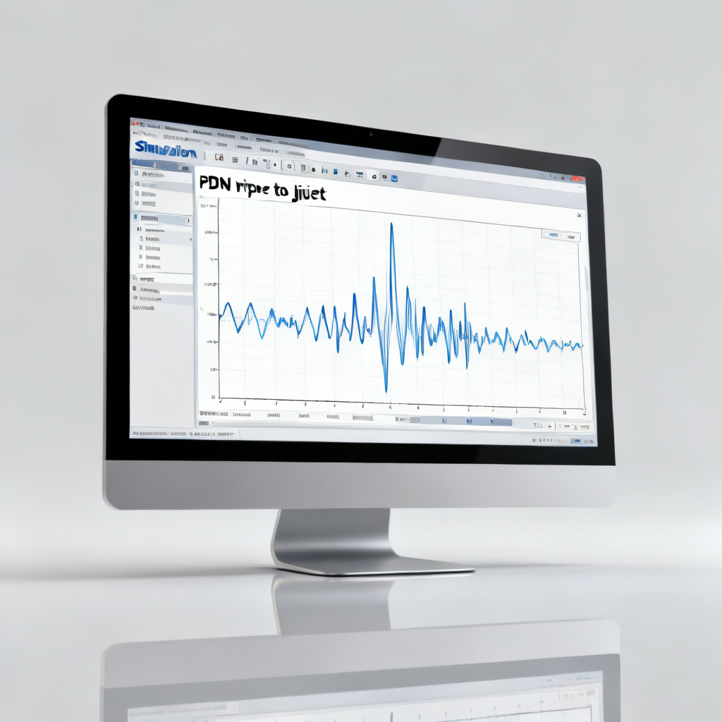
Measurement and Validation Techniques for Power Integrity
Designing for PI requires verification. Ripple and noise reduction techniques in power integrity PCB design rely on proper oscilloscope probing, VNA impedance measurement, and time-domain transient response analysis.
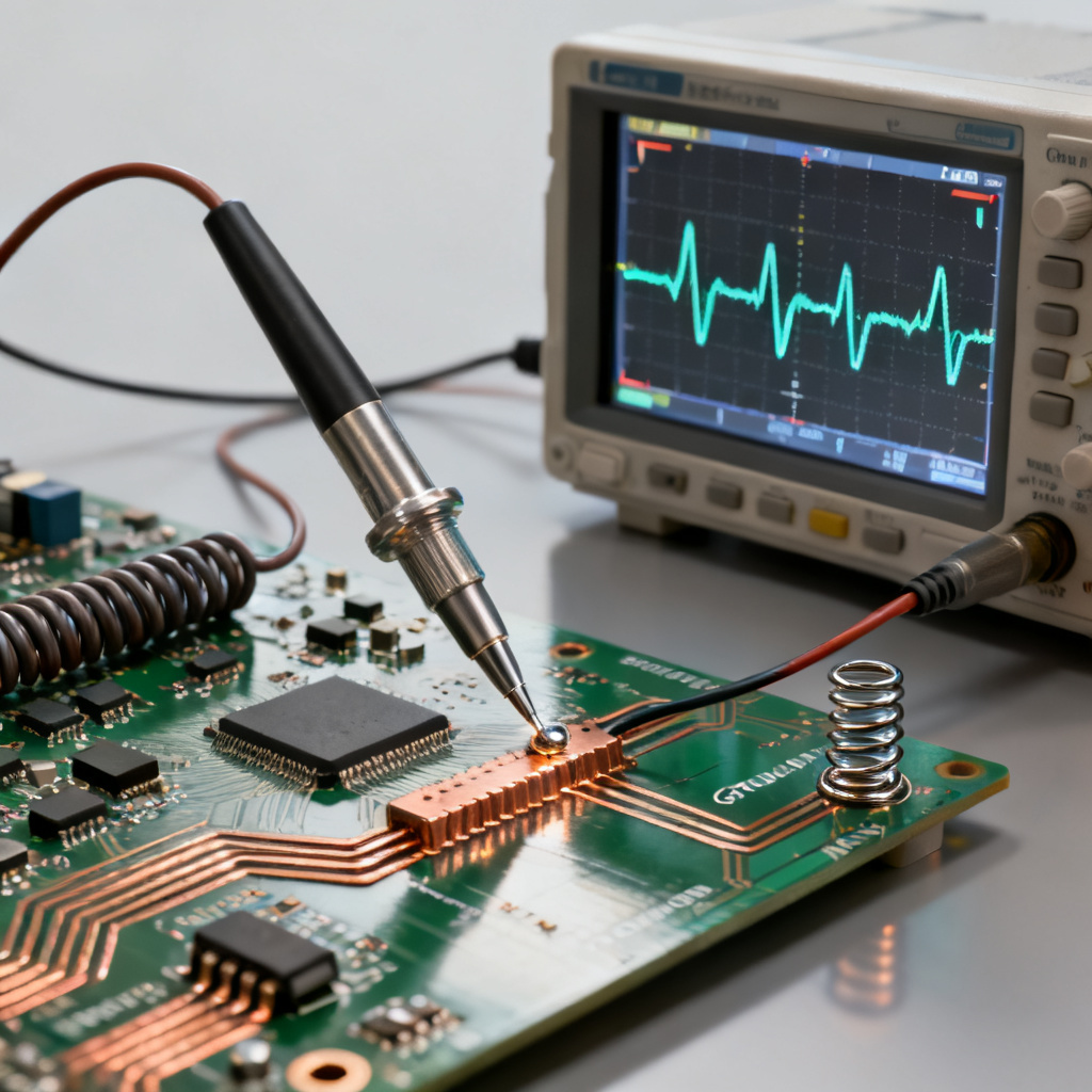
Proper Oscilloscope Probing
- Use a 1:1 passive probe (not 10:1) for low-voltage ripple measurements.
- Remove the probe ground lead and spring tip; use a ground spring or coaxial cable connection.
- Set oscilloscope to AC coupling and limit bandwidth (e.g., 20 MHz) to filter random high-frequency noise.
Measuring PDN Impedance with a VNA
A Vector Network Analyzer (VNA) measures PDN impedance from VRM to load. Inject a small AC signal through a low-inductance probe and measure reflected signal to calculate impedance vs. frequency. Look for anti-resonance peaks and ensure they are below Z_target.
Time-Domain Transient Response
Inject a current transient (e.g., 1A to 5A step) and observe voltage droop and ringing. The deviation must stay within ripple tolerance (e.g., ±3%). Add bulk capacitance for droop or improve high-frequency decoupling for ringing.
Practical Design Checklist for Ripple and Noise Reduction in High-Speed PCBs
| Step | Action | Key Parameter |
|---|---|---|
| 1 | Define PDN impedance target early | Z_target = (V_rail × ripple_tolerance) / I_transient |
| 2 | Use multi-layer stackup with adjacent power/ground planes | Thin dielectric (2–4 mils) |
| 3 | Place bulk capacitors at VRM output | 10 µF to 1000 µF |
| 4 | Place high-frequency bypass capacitors at each IC power pin | 1 nF to 100 nF, low ESL |
| 5 | Minimize loop inductance | Multiple vias, short traces, small anti-pads |
| 6 | Isolate analog and digital power rails | Ferrite beads or LDOs |
| 7 | Simulate PDN impedance profile | Ansys SIwave, Cadence Sigrity |
| 8 | Stitch ground planes with vias | 1 mm from every power via |
| 9 | Use proper probing techniques | 1:1 probe, ground spring, AC coupling |
| 10 | Incorporate filtering for sensitive rails | LC, π, or ferrite beads |
Frequently Asked Questions
What is the difference between ripple and noise in power integrity PCB design?
Ripple is periodic, low-frequency AC from switching regulators, while noise is high-frequency, non-periodic disturbances from digital switching, parasitic elements, and EMI. Ripple and noise reduction techniques in power integrity PCB design address both through decoupling, filtering, and layout optimization.
How do I calculate the target impedance for my PDN?
Target impedance is calculated as Z_target = (V_rail × ripple_tolerance) / I_transient. For example, a 1.0V rail with 3% ripple and 5A transient requires Z_target ≤ 6 mΩ. This guides ripple and noise reduction techniques in power integrity PCB design to maintain low impedance across all frequencies.
What is the best capacitor value for high-frequency decoupling?
For noise above 10 MHz, use small-value capacitors (1 nF to 100 nF) with very low ESL, such as 0402 or 0201 X7R. These are critical in ripple and noise reduction techniques in power integrity PCB design for bypassing high-frequency noise at IC power pins.
Why is via placement important for power integrity?
Vias introduce inductance that can create resonance and amplify noise. Ripple and noise reduction techniques in power integrity PCB design require multiple vias in parallel, minimized stub length, and small anti-pads to reduce via inductance and maintain low PDN impedance.
How do I measure ripple and noise on a power rail?
Use a 1:1 passive probe with a ground spring, AC coupling, and bandwidth limiting (e.g., 20 MHz). This ensures accurate measurement for validating ripple and noise reduction techniques in power integrity PCB design.