Split planes and slot antennas are hidden power integrity PCB problems that silently degrade high-speed PCB performance. This guide reveals how these structures create return path discontinuities and unintentional radiators, impacting signal integrity and EMI compliance.

Understanding Split Planes and Their Impact on Power Integrity
What Are Split Planes?
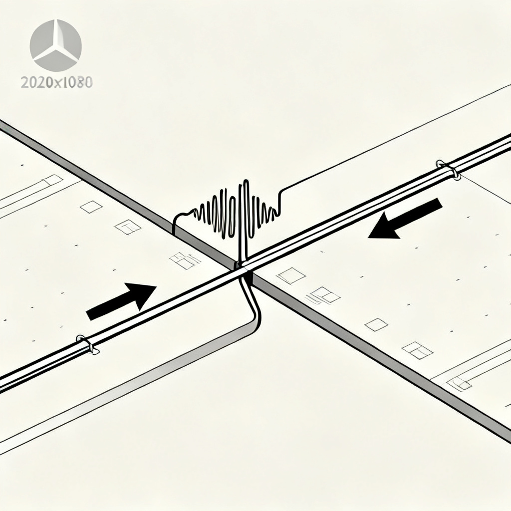
A split plane is a continuous copper layer (typically power or ground) that has been divided into separate, electrically isolated regions. This is commonly done to separate analog and digital power domains (e.g., AVCC and DVCC), isolate noisy switching currents from sensitive analog circuitry, or route signals across layers while maintaining clearance rules. However, when a signal trace crosses over a split in a reference plane, the return current cannot flow directly beneath it. This forces the current to find an alternative path—often through vias, capacitors, or the edges of the split—creating a large current loop that degrades power integrity.
The Return Current Problem
In high-speed designs, the return current flows in the reference plane directly beneath the signal trace (due to the principle of least inductance). When a trace crosses a split plane, the return current must detour around the split. This increases the loop area, which increases inductance and radiated emissions. The signal sees an impedance discontinuity, causing reflections and ringing. If the split is narrow (< 20 mils), the return current may still couple capacitively across the gap, but this is unreliable and frequency-dependent. For split widths > 50 mils, the coupling is negligible, and the return path becomes a major antenna. For example, a 100 MHz digital signal crossing a split in the ground plane can create a 5–10 dB increase in EMI, violating FCC/CE standards.
Why Split Planes Cause Power Integrity Degradation
Split planes create a discontinuity in the power distribution network (PDN). The PDN is designed to have low impedance across a wide frequency range. A split introduces a parasitic inductance and capacitance that can resonate, causing voltage droop at the IC supply pins, ground bounce due to simultaneous switching outputs (SSO), and power plane resonance that amplifies noise at specific frequencies. An engineering rule of thumb: never route high-speed signals across a split plane unless you provide a stitching capacitor (e.g., 0.1 µF or 10 nF) bridging the two planes. Even then, this is a band-aid, not a solution.
Slot Antennas—The Unintentional Radiators
What Is a Slot Antenna?
A slot antenna is a structure that behaves like a dipole antenna, but instead of a wire, it is an opening (slot) in a conductive plane. In PCBs, slot antennas are unintentionally created by long, narrow cutouts in ground or power planes (e.g., for isolation), gaps between copper pours (e.g., around connector mounting holes), rows of vias that create a “slot” in the plane (e.g., via fences that are not properly stitched), or slots in the reference plane caused by routing channels or differential pair gaps. A slot behaves as a resonant antenna when its length is close to an integer multiple of half the wavelength of the operating frequency. For a 2.4 GHz signal, a slot just 6.25 cm long can become a quarter-wave radiator.

How Slot Antennas Couple into Power Integrity
Slot antennas couple energy from the power/ground planes into free space, creating EMI. More critically, they also couple external noise back into the PDN, causing power supply ripple at the resonant frequency, desensitization of RF receivers, and bit errors in high-speed digital buses (e.g., DDR4, PCIe Gen 4). The coupling mechanism is electromagnetic. The slot acts as a transformer, converting plane-mode noise (common-mode) into radiated fields. The efficiency of this coupling depends on slot length (resonance condition), slot width (narrower slots have higher Q), and dielectric constant of the board material (higher εr lowers resonant frequency).
Real-World Example: The Connector Cutout Problem
A common mistake is creating a large cutout in the ground plane around a board-to-board connector (e.g., for high-voltage isolation or mechanical clearance). This cutout forms a slot antenna. When high-speed signals pass through the connector, the return current is forced around the slot, creating a large loop that radiates strongly at the slot’s resonant frequency. Near-field scanning with a spectrum analyzer often reveals a “hot spot” at the slot edges, corresponding to the resonant frequency of the cutout.
The Hidden Interaction—Split Planes Becoming Slot Antennas
When a Split Becomes an Antenna
A split plane is not just a DC obstacle; it is a slot. If the split is long and narrow (e.g., a 10 mm long, 1 mm wide gap in a ground plane), it will resonate at a frequency determined by its length. For a slot in free space, the resonant frequency (f) is approximately: f = c / (2L√εr), where c = speed of light (3×10⁸ m/s), L = slot length (meters), and εr = relative permittivity of the PCB material. For example, a 50 mm long slot in FR4 (εr ≈ 4.5) resonates at about 1.4 GHz—right in the middle of common wireless bands (LTE, Wi-Fi).
The Power Integrity Consequence
When a split plane resonates, it creates a high-impedance path for return currents at that frequency. This causes increased PDN impedance at the resonant frequency, voltage ripple at the IC power pins potentially exceeding the tolerance of the device (e.g., ±5% for 1.8V logic), and cross-talk between different power domains (e.g., digital noise coupling into the analog supply). The resonance also creates a virtual ground bounce at the slot edges, which can cause false triggering of logic gates or latch-up in sensitive CMOS ICs.
The “Hidden” Nature of the Problem
Unlike obvious SI issues (e.g., eye diagram closure), slot antenna effects are often subtle. They may only appear under specific operating conditions (e.g., when a particular frequency is present), can be mistaken for thermal noise or power supply ripple, and are difficult to simulate without full-wave 3D EM solvers (e.g., HFSS, CST). Many engineers assume that a split plane is “safe” if the signal trace is not crossing it. This is false. The split itself can couple energy from the power plane into the signal layer via fringing fields, especially at high frequencies (> 1 GHz).
Detection and Measurement Techniques
Pre-Layout Simulation
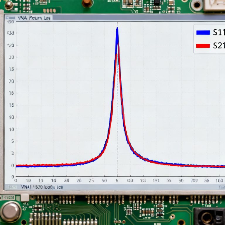
Use PDN analyzer tools to check for plane resonances. Set up a port across the split and compute the S-parameters. A sharp dip in S21 indicates a slot antenna resonance. Full-wave simulation is essential for complex geometries. Use eigenmode analysis to find the resonant frequencies of the plane-slot structure.
Post-Layout Verification
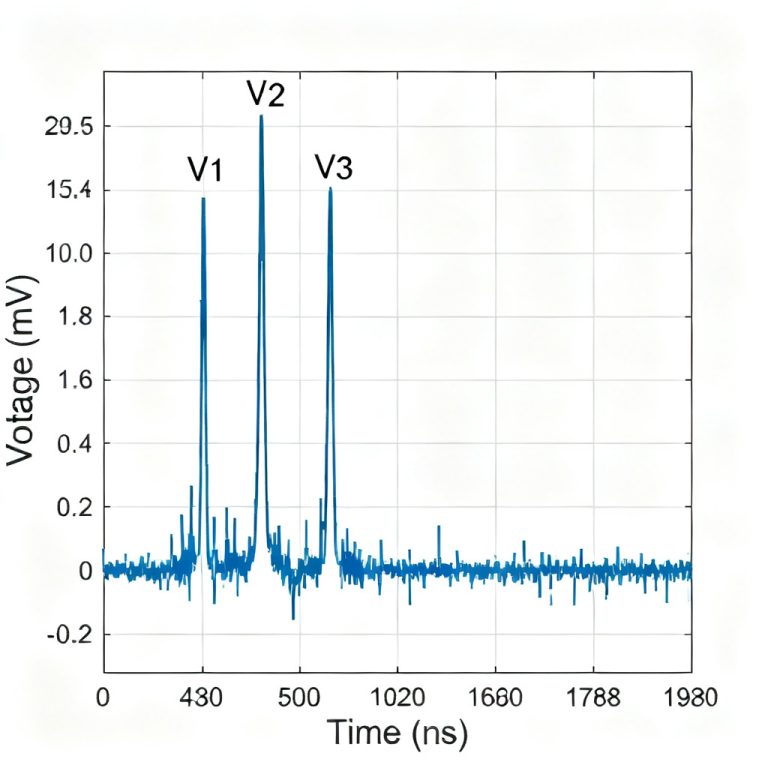
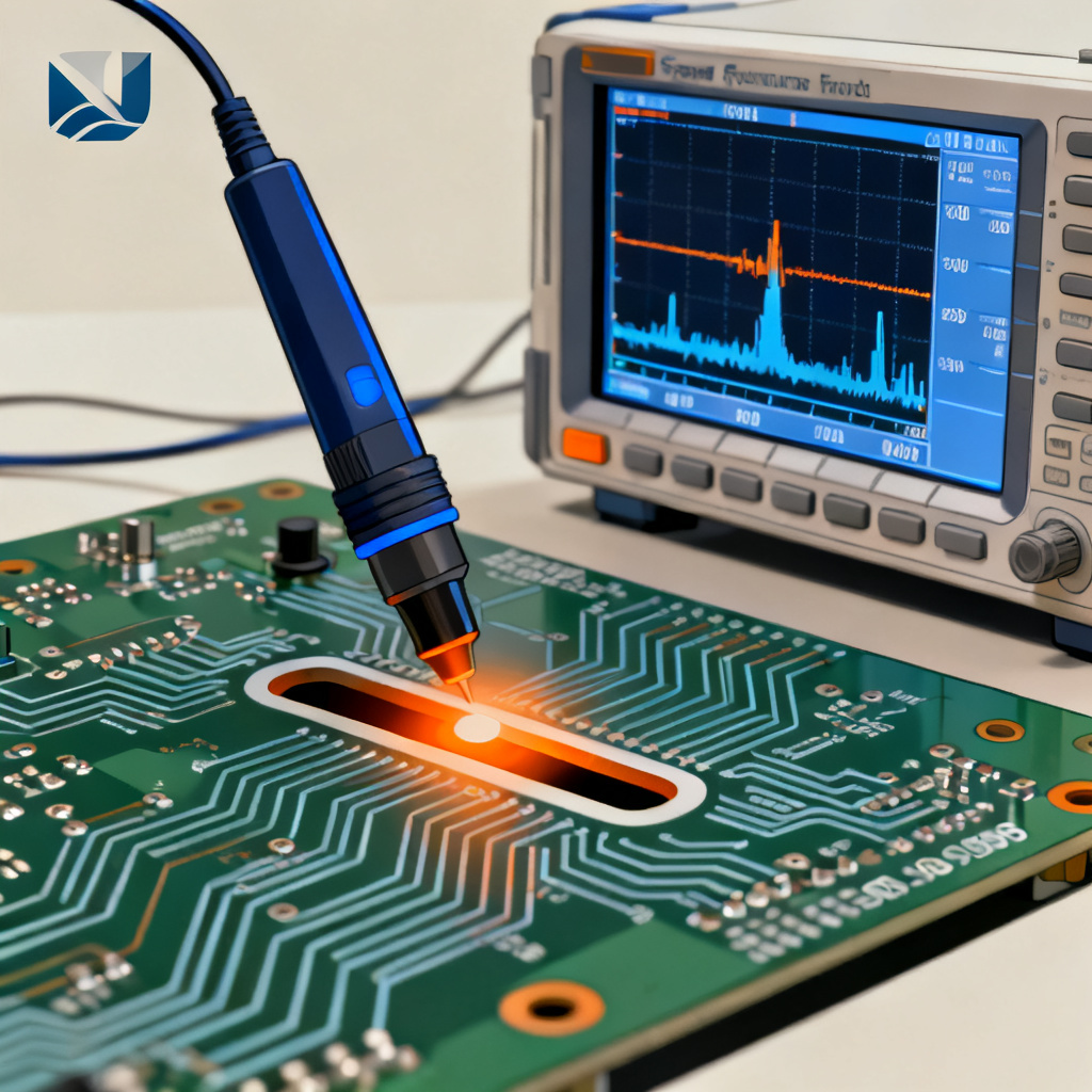
After fabrication, use TDR (Time Domain Reflectometry) to look for impedance discontinuities near splits. Use a VNA (Vector Network Analyzer) to measure S21 between two points on the plane. A notch in the transmission indicates a slot resonance. Use near-field probes to scan the board surface. A “hot spot” at the slot edges confirms radiation. If you see a 5–10 dB spike in the radiated emissions spectrum that matches the slot length calculation, you have a slot antenna problem.
Diagnostic Signatures
EMI peaks at frequencies corresponding to slot length, power supply ripple that changes with signal activity, unexplained bit errors in high-speed links (e.g., DDR, SerDes), and temperature-dependent performance (dielectric constant changes with temperature, shifting the resonant frequency).
Design Rules to Eliminate Split Plane and Slot Antenna Problems
Avoid Splits in Reference Planes
Never split a ground or power plane underneath a high-speed signal trace. If you must have multiple power domains, use a solid ground plane and route the power as separate traces or use a power island with a wide bridge. If a split is unavoidable (e.g., for isolation), provide a stitching capacitor (e.g., 0.1 µF or 10 nF) across the split, placed as close as possible to the signal crossing point. This provides a low-impedance return path for high frequencies.
Minimize Slot Length and Width
Keep any slot (cutout, gap, via row) shorter than 1/20th of the wavelength at the highest operating frequency. For a 10 GHz signal, this means slot length < 1.5 mm. If a slot is longer than 1/10th wavelength, break it into multiple smaller slots using stitching vias or copper bridges every 1/20th wavelength.
Use Stitching Vias Effectively
Stitching vias connect the ground plane on different layers, reducing the effective slot length. Place vias along the edges of any cutout or split, spaced no more than 1/10th wavelength apart. For a 2.4 GHz board, stitch vias every 5 mm along the slot. For 5 GHz, every 2.5 mm.
Optimize Plane Layer Stackup
Use a solid ground plane adjacent to the signal layer. Avoid using power planes as the reference for high-speed signals unless necessary. If using a split power plane, ensure the ground plane is continuous and unbroken. The ground plane should be the closest reference plane to the signal layer.
Avoid Connector Cutout Antennas
For board-to-board connectors, avoid large cutouts in the ground plane. If a cutout is required for mechanical reasons, fill the area with ground vias around the perimeter to create a “via fence” that suppresses slot radiation. Use grounded coplanar waveguide (GCPW) routing for high-speed signals near connectors. This provides a controlled impedance path and a continuous ground reference.
Simulation and Verification
Always run a power integrity simulation (e.g., using Ansys SIwave or Cadence Sigrity) to check for plane resonances and slot antenna effects. After fabrication, perform EMI pre-compliance testing with a near-field probe to catch slot antenna problems before final certification.
Case Study—A Real-World Split Plane Failure
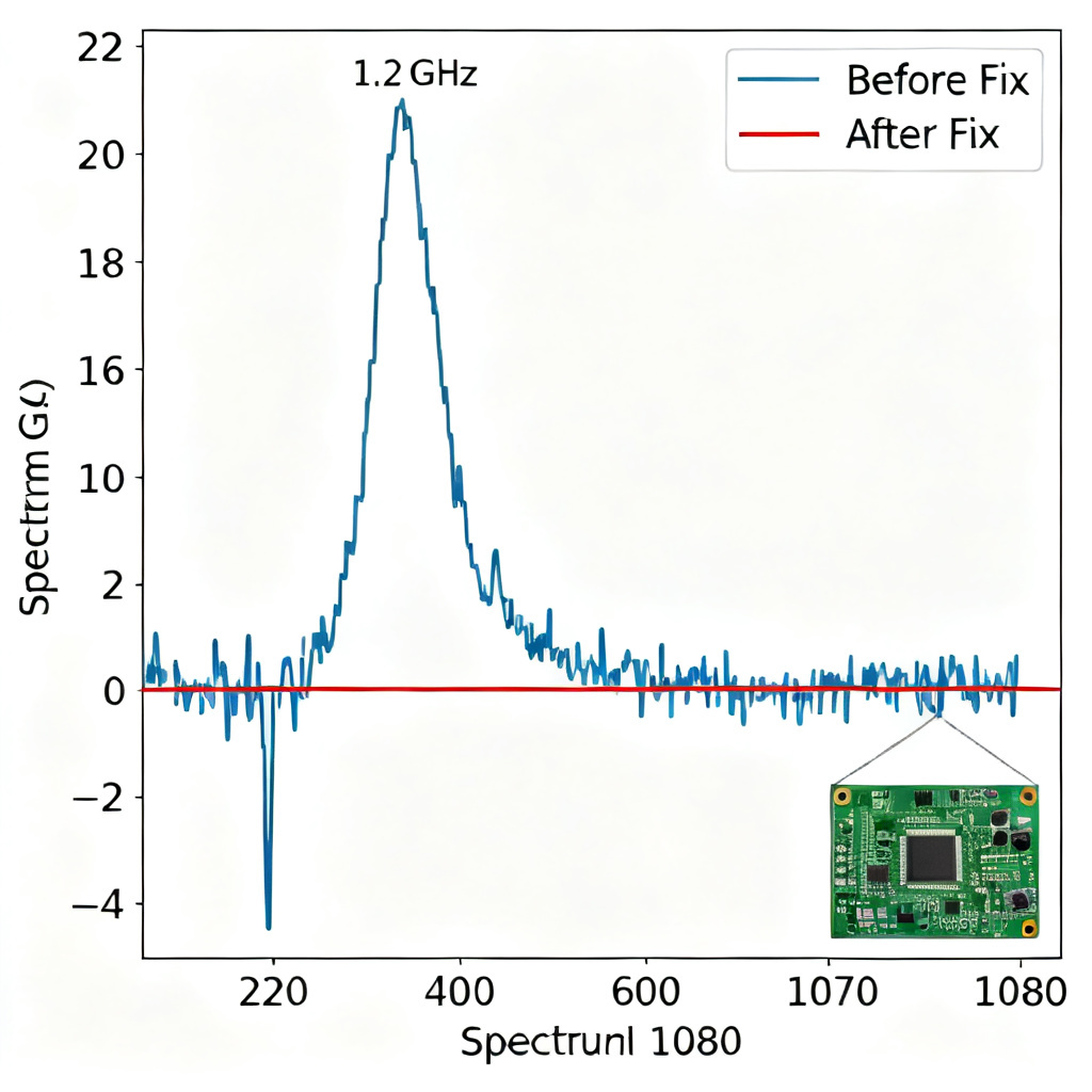
Scenario: A high-speed digital board (10-layer, 0.062″ thick, FR4) with a split ground plane separating analog and digital sections. A 1.5 Gbps LVDS signal crossed the split. The board failed FCC Class B radiated emissions at 1.2 GHz.
Root Cause Analysis: The split length was 45 mm. Resonant frequency calculation: f = c / (2L√εr) = 3×10⁸ / (2 × 0.045 × √4.5) ≈ 1.25 GHz. The LVDS signal had a 1.2 GHz component due to the data pattern. The split acted as a slot antenna, radiating strongly at 1.2 GHz.
Solution: Added a 0.1 µF stitching capacitor across the split, placed within 5 mm of the LVDS trace crossing. Added 10 stitching vias along the split edge, spaced 4 mm apart. Re-routed the LVDS trace to avoid crossing the split entirely (using a ground via transition).
Result: Radiated emissions dropped by 12 dB at 1.2 GHz, passing FCC Class B.
Summary and Best Practices for B2B Procurement
For B2B PCB buyers and engineers, understanding these hidden problems ensures you receive boards that perform reliably in high-speed applications.
Key Takeaways for Procurement: Specify a continuous ground plane in your stackup requirements. Avoid “split ground” unless absolutely necessary. Request a PDN simulation report from your PCB manufacturer or design partner, especially for boards with multiple power domains. Ask about via stitching on any large cutouts or slots. A good manufacturer will suggest stitching vias automatically. Review the gerber files for long, narrow gaps in copper planes. If you see a slot longer than 5 mm, flag it for review.
Key Takeaways for Engineers: Treat every split plane as a potential slot antenna. Use stitching vias and capacitors as your first line of defense. Simulate early, verify late. Never assume a split is “safe” just because no signal crosses it.
Final Thought: In high-speed PCB design, the most dangerous problems are the ones you cannot see. Split planes and slot antennas are invisible to the eye but devastating to performance. By understanding their behavior and applying the design rules above, you can eliminate these hidden power integrity problems and deliver boards that work right the first time.
Frequently Asked Questions about Split Planes and Slot Antennas
What are split planes and slot antennas in high-speed PCB design?
How do split planes cause power integrity degradation?
What design rules prevent slot antenna problems in PCBs?
| Parameter | Specification | Impact on Power Integrity |
|---|---|---|
| Split Plane Length | < 1/20th wavelength at highest frequency | Reduces slot antenna resonance |
| Stitching Via Spacing | 1/10th wavelength | Suppresses return path discontinuity |
| Stitching Capacitor Value | 0.1 µF or 10 nF | Provides low-impedance return path |
| Ground Plane Continuity | Solid, unbroken | Maintains low PDN impedance |