Master Power Integrity PCB Analysis for high-speed designs. This step-by-step guide covers DC IR drop, AC PDN impedance, decoupling capacitor optimization, and plane resonance simulation using Keysight ADS. A robust Power Integrity (PI) strategy ensures every active component receives clean, stable voltage across all frequencies, preventing failures in high-speed digital and RF PCBs. This professional workflow guarantees first-pass success for your high-speed PCB projects.
Step 1: DC IR Drop Analysis for Power Integrity PCB
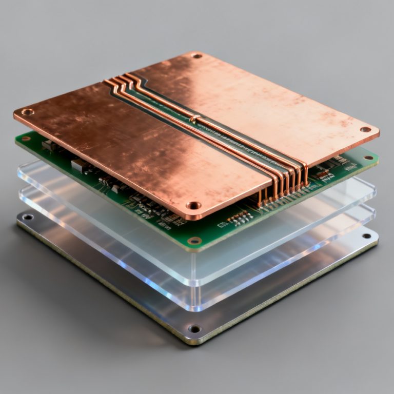
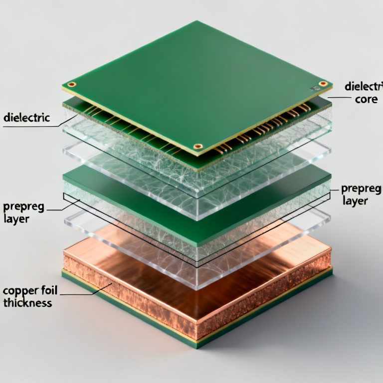
Setting up your PCB design for Power Integrity PCB Analysis begins with importing your layout in ODB++ format for accurate stackup and net information. Define the layer stackup with dielectric constant (Dk 4.2-4.5 for FR4), loss tangent (Df 0.02), copper thickness (1-2 oz), and dielectric thickness (4 mils recommended for low PDN impedance). Identify critical nets like VDD_CORE (1.0V) and the IC load with its transient current profile.
DC Simulation Controller Setup
Insert a DC Simulation controller, place a P_1Tone port at the VRM output (1.0V), and use current sink components at BGA balls to model IC DC current draw (e.g., 10A total). Run the simulation to generate voltage contour plots showing gradient from VRM to IC, and current density plots revealing hot spots. Verify IR drop: voltage at IC pins must remain within ±3% tolerance (0.970V to 1.030V). If voltage drops to 0.950V, increase copper thickness, widen power traces, or add more vias.
Step 2: AC PDN Impedance Profiling for Power Integrity PCB
Calculate target impedance using Z_target = (VDD * Ripple_Tolerance) / I_transient. For VDD=1.0V, ripple=5%, I_transient=5A, Z_target=10 mOhms. Set up AC simulation by deleting DC sources, placing a single P_1Tone port at the IC load location (50 Ohm impedance), and adding a VRM model with 1 mOhm resistor and 1 nH inductor. Insert an AC simulation controller with frequency sweep from 10 Hz to 1 GHz (log scale, 1000 points/decade). Model decoupling capacitors as series RLC circuits using S-parameter models from manufacturers (e.g., Murata, TDK) with ESR=5 mOhm and ESL=0.5 nH, plus mounting inductance (0.5-1 nH per via).
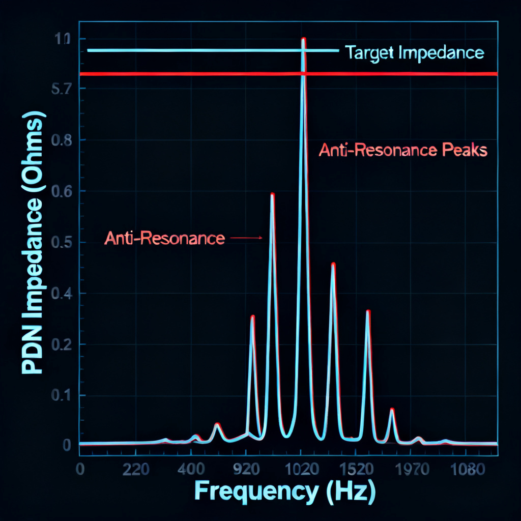
Analyzing Z(f) Plot for Power Integrity PCB
Plot Z(1,1) magnitude in Ohms. Low frequency (DC-10 kHz) is dominated by VRM. Mid frequency (10 kHz-10 MHz) shows capacitor valley with anti-resonance peaks. High frequency (10 MHz-1 GHz) rises due to plane inductance. Red flags include anti-resonance peaks above Z_target (fix by adding mid-frequency capacitors like 10nF or 1nF) and high inductive slope above 100 MHz (fix by moving high-frequency capacitors closer to IC pins or using thinner dielectric).
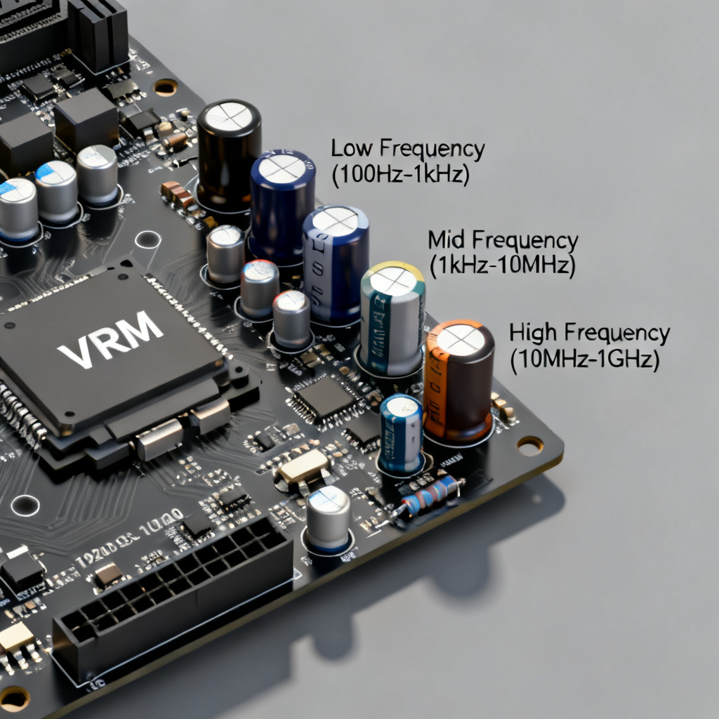
Step 3: Decoupling Capacitor Optimization for Power Integrity PCB
Use the three-bucket approach: bulk capacitors (10uF-100uF, electrolytic/tantalum) for low-frequency transients (10 kHz-1 MHz) near VRM; mid-frequency capacitors (0.1uF-1uF, MLCC) for mid-range (1 MHz-10 MHz) near IC; high-frequency capacitors (0.01uF-0.1uF, small MLCC 0402/0201) for high-frequency switching (10 MHz-100 MHz) as close as possible to IC power pins. In Keysight ADS, create design variables for capacitor values, set optimization goal Z(1,1) < 10 mOhms from 10 kHz to 1 GHz, and run the optimizer (Gradient or Random).
Simulation-Based Optimization Results
| Power Integrity PCB Parameter | Value |
|---|---|
| Target Impedance (Z_target) | 10 mOhms |
| Bulk Capacitors | 10uF-100uF, near VRM |
| Mid-Frequency Capacitors | 0.1uF-1uF, near IC |
| High-Frequency Capacitors | 0.01uF-0.1uF, at IC pins |
| ESR per Capacitor | 5 mOhm |
| ESL per Capacitor | 0.5 nH |
| Mounting Inductance per Via | 0.5-1 nH |
Key insight: fewer, larger-value capacitors placed correctly outperform many small ones. Over-crowding creates unwanted resonances.
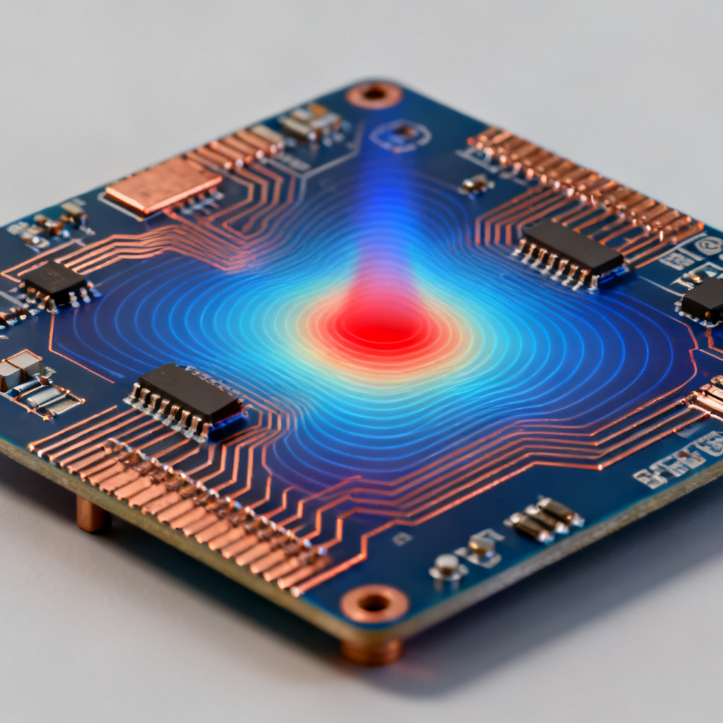
Step 4: Plane Resonance Simulation for Power Integrity PCB
Use Keysight Momentum RF or FEM simulator for cavity resonance analysis. Define power and ground plane layers as a stackup, place a port at the IC location, run frequency sweep from 100 MHz to 2 GHz, and plot E-field and H-field distribution at resonance frequencies. Look for areas of high E-field (voltage peaks) where the IC may experience noise. Apply stitching vias (ground vias connected to ground plane) or decoupling capacitors at resonance locations to dampen standing waves. A common technique is adding a 10pF “resonance killer” capacitor at the board center.
Step 5: Transient Simulation for Power Integrity PCB
Create a transient current profile using a PWL current source (0-10 ns: 0A to 5A; 10-20 ns: 5A to 1A; 20-30 ns: spike to 10A). Insert a Transient Simulation controller with time step of 1 ps. Plot voltage at the IC power pin over time. Look for voltage droop below minimum (0.970V), voltage overshoot above maximum (1.030V), and settling time within nanoseconds. If voltage droop is severe, add more bulk capacitance or reduce inductance of the decoupling path.
FAQ: Power Integrity PCB Analysis with Keysight ADS
What is the most critical step in Power Integrity PCB Analysis?
The AC PDN impedance profiling (Z(f) plot) is the most critical step in Power Integrity PCB Analysis because it reveals anti-resonance peaks and inductive slopes that directly impact high-speed performance.
How do I calculate target impedance for Power Integrity PCB?
Use Z_target = (VDD * Ripple_Tolerance) / I_transient. For a 1.0V rail with 5% ripple and 5A transient current, Z_target is 10 mOhms.
What decoupling capacitor strategy works best for Power Integrity PCB?
The three-bucket approach (bulk, mid-frequency, high-frequency) with simulation-based optimization using Keysight ADS ensures the PDN impedance stays below Z_target across all frequencies.
Why is plane resonance important in Power Integrity PCB Analysis?
Plane resonance creates voltage hot spots and cold spots across the board, causing noise at the IC. Simulation identifies these locations for targeted damping with stitching vias or capacitors.
What tools in Keysight ADS are used for Power Integrity PCB Analysis?
DC simulation for IR drop, AC simulation for PDN impedance, Momentum RF/FEM for plane resonance, and Transient simulation for dynamic performance are all essential tools.