Power integrity PCB pre-compliance is a critical self-check process for high-speed designs that prevents costly lab failures. By verifying power distribution network (PDN) performance before formal testing, engineers can ensure voltage stability and reduce expensive redesigns.
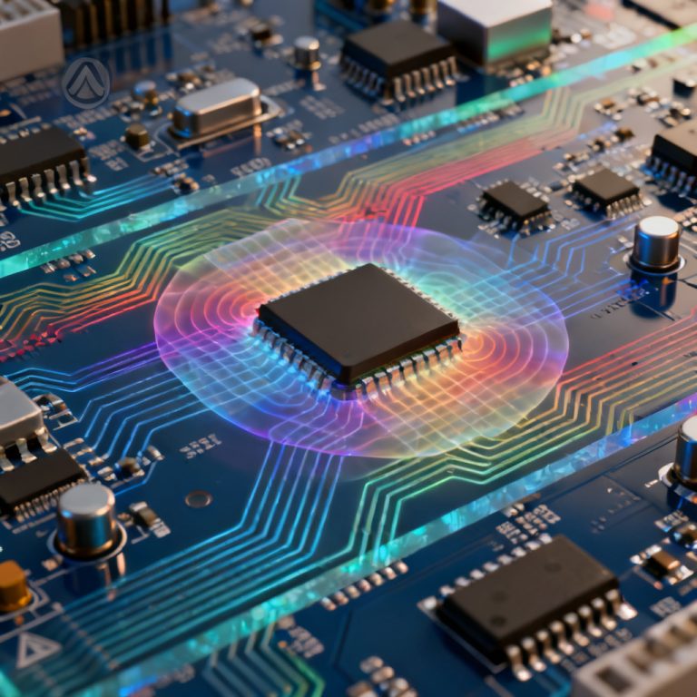
In high-speed PCB design, power integrity (PI) is no longer an afterthought—it is a critical factor that determines signal integrity, electromagnetic compatibility (EMC), and overall system reliability. For B2B printed circuit board manufacturers and designers, failing to address PI issues before formal lab testing can lead to expensive respins, delayed time-to-market, and lost customer trust.
Pre-compliance self-checking is the process of verifying power distribution network (PDN) performance using simulation tools, analytical calculations, and rule-based checks before sending a design to a certified lab for formal testing (e.g., impedance measurements, ripple noise tests). This guide merges expert insights from three leading sources to provide a step-by-step, no-nonsense approach to self-checking your PCB’s power integrity.
1. Understand the Core Power Integrity Metrics
Before any self-check, you must define what “good” power integrity PCB looks like. Based on industry best practices, focus on these key parameters:
1.1 Target Impedance (Z_target)
The PDN must maintain a low impedance across a wide frequency range (typically DC to several GHz). The target impedance is calculated as:
Z_target = (V_DD × Ripple Tolerance) / ΔI
Where: V_DD = Supply voltage (e.g., 1.2V), Ripple Tolerance = Typically 5% of V_DD (e.g., 60 mV for 1.2V), ΔI = Maximum transient current (e.g., 5A).
Self-Check Tip: Use a spreadsheet or simulation tool to compute Z_target for each power rail. If your PDN impedance exceeds this value at any frequency, you risk voltage droop and noise.
1.2 DC IR Drop
DC IR drop is the voltage loss due to resistance in traces, vias, and planes. A drop exceeding 3-5% of the nominal voltage can cause logic failures.
Self-Check Tip: Perform a DC simulation (e.g., using Ansys SIwave, HyperLynx, or free tools like LTSpice) to map voltage distribution. Check that the voltage at the load (e.g., FPGA core) is within tolerance.
1.3 AC Impedance and Resonances
At high frequencies, the PDN behaves as a distributed RLC network. Parallel resonances between decoupling capacitors and plane inductance can cause impedance spikes.
Self-Check Tip: Run an AC impedance sweep from 10 kHz to 1 GHz. Look for peaks above Z_target and note the frequency—this is where you need to add or adjust decoupling capacitors.
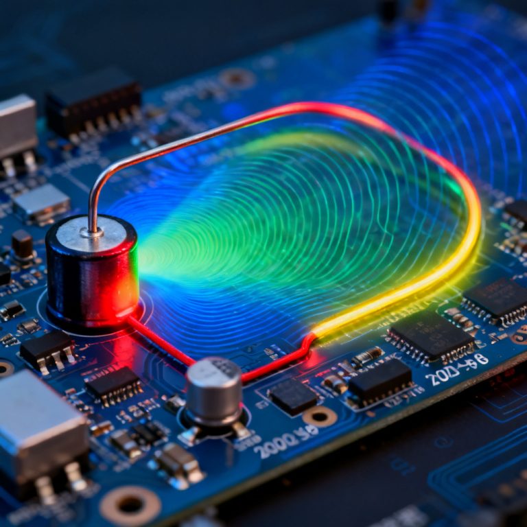
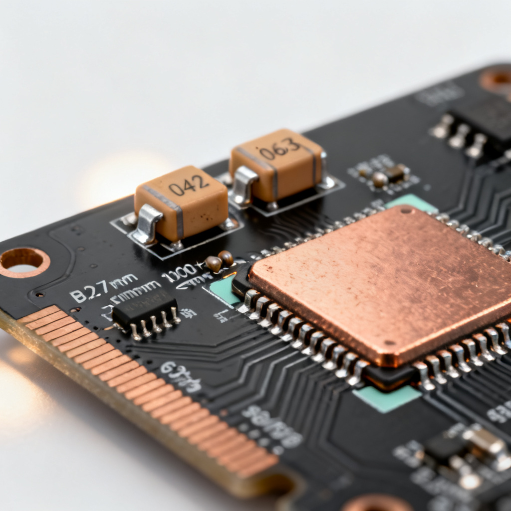
2. Perform a Power Integrity PCB Decoupling Capacitor Audit
Decoupling capacitors are the first line of defense against power noise. However, improper selection or placement renders them ineffective.
2.1 Capacitor Selection Based on Self-Resonant Frequency (SRF)
Each capacitor type has a self-resonant frequency where its impedance is lowest. For example: 100 nF (0402) SRF ~ 100 MHz, 10 µF (0603) SRF ~ 10 MHz, Bulk capacitors (100 µF) SRF ~ 1 MHz.
Self-Check Tip: Use a capacitor library (e.g., Murata SimSurfing or KEMET K-SIM) to verify SRF. Ensure you have a mix of values to cover the entire frequency band from 1 MHz to 1 GHz.
2.2 Placement and Via Inductance
Capacitors must be placed as close as possible to the power pins of the IC to minimize loop inductance. A common mistake is placing decaps more than 1 cm away, which adds parasitic inductance and reduces effectiveness.
Self-Check Tip: In your PCB layout tool, measure the distance from each decap to its target IC pin. If > 5 mm, consider moving it. Also, use short, wide traces (or direct via connections) to reduce inductance.
2.3 Anti-Resonance Checks
When multiple capacitor values are used, anti-resonance peaks can occur at frequencies where one capacitor’s inductive region meets another’s capacitive region.
Self-Check Tip: Simulate the combined impedance of all decaps for a given power rail. If you see a spike above Z_target, adjust the number or value of capacitors. A common fix is to add a “spreader” capacitor (e.g., 1 µF) between two values.
3. Evaluate Plane and Via Design for Power Integrity PCB
Power and ground planes form the backbone of the PDN. Poor plane design introduces inductance and resistance.
3.1 Plane Pair Capacitance
The intrinsic capacitance between a power and ground plane provides high-frequency decoupling. For a 4-layer stackup with a 0.1 mm dielectric: Capacitance per square inch ≈ 10 pF.
Self-Check Tip: Calculate the total plane capacitance for each power rail. If it is less than 10% of the total required decoupling capacitance, consider increasing plane area or reducing dielectric thickness.
3.2 Via Inductance and Stitching
Vias connecting planes add inductance (typically 0.5-1 nH per via). Multiple vias in parallel reduce effective inductance.
Self-Check Tip: Use at least two vias per decoupling capacitor pad (one for power, one for ground) and ensure they are close together. For high-current rails (e.g., 10A+), add stitching vias along the plane edges to reduce impedance.
3.3 Plane Cutouts and Splits
Avoid splitting power planes under high-speed ICs. A split plane forces return currents to take a longer path, increasing inductance and causing voltage noise.
Self-Check Tip: In your layout, check for any gaps or slots in the power plane under critical components (e.g., FPGAs, DDR memory). If unavoidable, add stitching capacitors across the split.
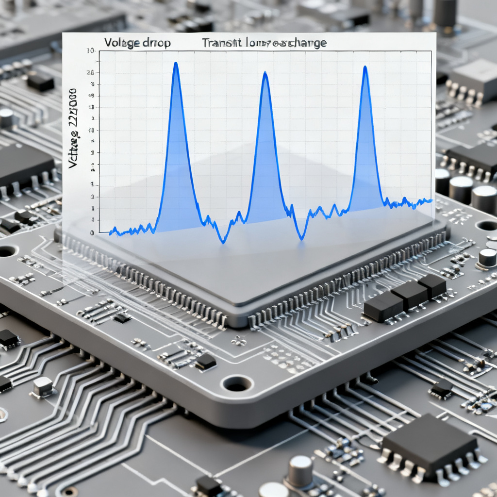
4. Conduct a Transient Load Simulation for Power Integrity PCB
Real-world ICs draw current in bursts (e.g., during clock edges or data bus switching). This transient current causes voltage droop if the PDN cannot respond quickly.
4.1 Step Load Response
Simulate a step change in current (e.g., from 0A to 5A in 1 ns) and observe the voltage at the load.
Self-Check Tip: Use a time-domain simulation (e.g., with LTSpice or Cadence Sigrity). Look for voltage droop below the allowed tolerance (e.g., 1.14V for a 1.2V rail). If droop exceeds tolerance, add more bulk capacitance or reduce inductance.
4.2 Ripple and Noise Measurement
Even with good DC performance, high-frequency ripple from switching regulators can couple into sensitive analog or RF circuits.
Self-Check Tip: Place a virtual probe at the load and run a transient simulation with the actual power supply model (including switching frequency and output ripple). Ensure the ripple amplitude is below the component’s noise margin (e.g., < 10 mV for high-speed ADCs).
5. Use Low-Cost Pre-Compliance Tools for Power Integrity PCB
You don’t need a $100,000 VNA to perform pre-compliance. These tools offer sufficient accuracy for self-checks:
5.1 Oscilloscope with FFT
A 4-channel oscilloscope (e.g., 500 MHz bandwidth) with FFT capability can measure power rail ripple and noise.
Self-Check Tip: Use a 50-ohm probe with a DC blocking capacitor to measure AC noise on the power rail. Set the FFT to average mode and look for spikes at the switching frequency of the regulator (e.g., 1 MHz, 10 MHz).
5.2 VNA for Impedance Measurement (Optional)
A low-cost vector network analyzer (e.g., NanoVNA) can measure PDN impedance from 10 kHz to 1 GHz if calibrated with a custom fixture.
Self-Check Tip: Create a 2-port shunt-through fixture using SMA connectors. Measure S21 and convert to impedance. Compare with simulation results.
5.3 Free Simulation Software
- LTSpice: Ideal for transient and AC analysis of decap networks.
- KiCad with NGSPICE: For basic PDN simulations.
- OpenEMS: For 3D electromagnetic field simulation (advanced).
Self-Check Tip: Always cross-verify simulation results with at least one measurement (e.g., DC IR drop using a multimeter) to build confidence.
6. Document and Iterate Your Power Integrity PCB Self-Check
Pre-compliance is not a one-time event. Create a checklist and document all findings:
6.1 Power Integrity PCB Pre-Compliance Checklist
| Check Item | Power Integrity PCB Parameter | Status |
|---|---|---|
| Target impedance | Calculated for all rails | □ |
| DC IR drop | < 3% at worst-case load | □ |
| Decap SRF | Covers 1 MHz to 1 GHz | □ |
| Anti-resonance peaks | No peaks above Z_target | □ |
| Plane capacitance | > 10% of total decap requirement | □ |
| Via inductance | Minimized (multiple vias per decap) | □ |
| Plane splits | No splits under critical ICs | □ |
| Transient droop | Within tolerance | □ |
| Ripple noise | Below component specification | □ |
6.2 When to Go to Lab Testing
Only after passing all self-checks should you proceed to formal lab testing (e.g., VNA impedance measurement, noise spectrum analysis, EMC pre-scan). The lab will validate your design and catch any second-order effects (e.g., crosstalk between planes, thermal effects).
FAQ: Power Integrity PCB Pre-Compliance
What is power integrity PCB pre-compliance?
Power integrity PCB pre-compliance is the process of self-checking your design’s power distribution network using simulation and analysis before formal lab testing, ensuring voltage stability and reducing redesign risks.
Why is target impedance important for power integrity PCB?
Target impedance defines the maximum allowable PDN impedance across frequency; exceeding it causes voltage droop and noise in high-speed circuits.
How do I check decoupling capacitor placement for power integrity PCB?
Measure the distance from each capacitor to its target IC pin—keep it under 5 mm and use short, wide traces to minimize loop inductance.
What tools are recommended for power integrity PCB self-check?
Use free simulation software like LTSpice, an oscilloscope with FFT, and a low-cost VNA for impedance measurement.
Comparison: Power Integrity PCB Self-Check vs. Lab Testing
| Aspect | Power Integrity PCB Self-Check | Lab Testing |
|---|---|---|
| Cost | Low (free tools, basic equipment) | High (certified lab fees) |
| Speed | Immediate results during design | Days to weeks turnaround |
| Accuracy | Sufficient for pre-compliance | High (certified measurements) |
| Flexibility | Iterative, easy to modify | One-time validation |
| Risk of failure | Reduced by 70-80% | Full detection |
Our service combines rigorous self-check support with high-speed PCB manufacturing, helping you achieve first-pass success without compromising quality.
Key Terminology for Power Integrity PCB
- PDN (Power Distribution Network): The network of planes, traces, and vias delivering power to ICs.
- Decoupling Capacitor: A capacitor placed near ICs to supply transient current and filter noise.
- Self-Resonant Frequency (SRF): The frequency at which a capacitor’s impedance is minimum due to its internal inductance.
- Anti-Resonance: A high-impedance peak caused by interaction between multiple capacitor values.
- IR Drop: Voltage loss due to resistance in the PDN.