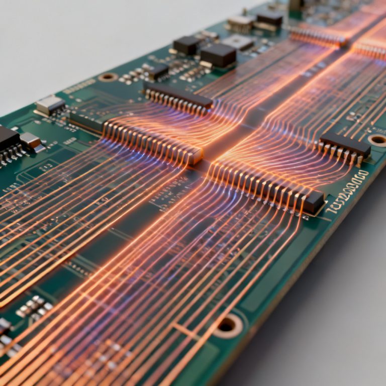
Vias are the most critical and uncontrollable part of high-speed PCB signal paths. Acting as a combination of parasitic capacitance, inductance, and redundant stub segments, poorly designed vias cause signal attenuation, resonance, jitter, and impedance discontinuity—especially for 10Gbps+, 25Gbps SerDes, PCIe, and DDR high-speed applications. Mastering high speed PCB via design is essential for every hardware engineer.
This ultimate pillar guide covers all via types, stub resonance mechanism, back drilling principles and specifications, impedance optimization parameters, layout placement rules, signal-specific requirements, and a complete design checklist. As covered in our PCB Design Guidelines, proper high speed PCB via design directly impacts signal integrity and manufacturing yield.
Table of Contents
- 1. Why Via Design Matters in High-Speed PCB
- 2. PCB Via Types, Pros Cons & Application Scenarios
- 3. Via Stub Effect: Mechanism, Resonance & Speed-Level Impact
- 4. Back Drilling Technology: Principle, Design Parameters & Mandatory Usage Scenarios
- 5. High-Speed PCB Via Impedance Optimization Guidelines
- 6. Universal Via Placement Rules for High-Speed Signals
- 7. Via Design Requirements by Signal Type (PCIe/DDR/SerDes/Clock)
- 8. High-Speed Via Design Complete Checklist
- 9. Key Takeaways
- 10. FAQ About High-Speed PCB Via Design
- 11. Professional Via Design Review & Back Drilling Feasibility Consultation
Why Via Design Matters in High-Speed PCB
In multilayer high-speed PCBs, routing layer transitions inevitably rely on vias, which become the weakest and most uncontrollable link in the entire signal integrity chain. Understanding high speed PCB via design is critical for any engineer working with gigabit interfaces. Unlike low-speed designs where vias can be treated as simple connections, high-speed applications demand precise control of every via parameter.
Electrically, a standard PCB via is not just a simple conductive connection—it behaves as an integrated equivalent circuit composed of parasitic capacitance + parasitic inductance + unused copper stub. At low signal rates below 5Gbps, these parasitic effects can be ignored; however, once the data rate reaches 10Gbps and above, tiny via structure defects will trigger severe signal reflection, insertion loss, crosstalk, and timing jitter.
For modern high-end applications including PCIe 4.0/5.0, 25Gbps+ SerDes, 100G Ethernet, and DDR5 memory interfaces, via design details directly determine system stability, signal margin, and product yield. Unreasonable via layout cannot be compensated by later routing tuning, making standardized high speed PCB via design a fundamental requirement for reliable SI layout.
PCB Via Types, Pros Cons & Application Scenarios
Choosing the correct via type is the first step of high-speed design, balancing fabrication cost, process capability, stub length, density, and high-frequency performance. The four mainstream via types are through-hole via, blind via, buried via, and HDI microvia, each with clear advantages, disadvantages, and applicable speed ranges. For detailed HDI and microvia application in BGA fanout, see our BGA Fanout Techniques Guide.
| Via Type | Core Advantages | Key Disadvantages | Best Application Scenarios |
|---|---|---|---|
| Through-Hole Via | Low cost, mature fabrication, wide compatibility | Long via stub, large parasitic effect | ≤5Gbps low-to-medium speed signals |
| Blind Via | Short stub length, minimal unused copper | Higher cost, limited layer span | 5–15Gbps signals, BGA fanout |
| Buried Via | Saves routing space, clean surface layout | Complex process, higher cost | High-density multilayer PCB |
| HDI Microvia | Ultra-small size, ultra-short stub, high density | Premium cost, strict process | 15Gbps+ signals, fine-pitch BGA |
Professional Tip: For 15Gbps and above high-speed designs, HDI microvia is preferred to reduce parasitic parameters and avoid stub resonance fundamentally. This is a key principle of advanced high speed PCB via design.
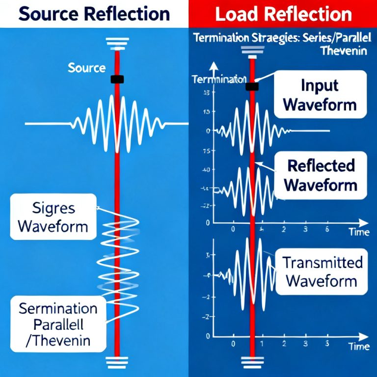
Via Stub Effect: Mechanism, Resonance & Speed-Level Impact
What Is Via Stub Effect
A via stub refers to the redundant unused copper barrel segment of a via that does not connect to any signal layer after layer transition. This leftover copper forms an open-circuited resonant structure, creating fixed-frequency resonance notches that severely attenuate high-speed signal energy—it is widely regarded as the hidden signal killer in high-speed PCB design. Proper high speed PCB via design must address stub effect above 10Gbps.
Resonance Frequency Calculation
The via stub resonant frequency follows the classic engineering formula:
f_res ≈ 1 / (4 × T_stub × Velocity_factor)Shorter stub length pushes the resonant frequency higher, moving it outside the working bandwidth and avoiding signal interference. Longer stubs lower the resonant frequency, directly overlapping with 10G/25G signal bandwidth and causing severe performance degradation. The stackup that determines stub length is covered in our Stackup Design Guide, which works hand-in-hand with high speed PCB via design.
Signal Rate vs Stub Impact Level
| Signal Speed | Stub Effect Influence | Design Recommendation |
|---|---|---|
| ≤5Gbps | Negligible impact | No special stub treatment required |
| 5–10Gbps | Slight signal degradation | Control stub length strictly |
| 10–25Gbps | Obvious loss and resonance | Back drilling strongly recommended |
| 25Gbps+ | Severe signal collapse | Back drilling mandatory |
Back Drilling Technology: Principle, Design Parameters & Mandatory Usage Scenarios
Working Principle of Back Drilling
Back drilling is a specialized PCB post-fabrication process that uses secondary precision drilling to remove the redundant copper barrel of via stubs. It cuts off the open resonant structure, eliminates stub parasitic interference, and is the most mature, cost-effective solution for solving via stub problems in industry. When combined with proper Impedance Matching Ultimate Guide practices, back drilling ensures continuous impedance through via transitions — a critical aspect of high speed PCB via design.
Standard Back Drilling Design Parameters
| Key Parameter | Industrial Standard Requirement |
|---|---|
| Remaining Stub Length After Drilling | 5–10 mil |
| Back Drilling Depth Tolerance | ±0.05mm |
| Standard Process Layer Range | 1–6 layers conventional back drilling |
When Back Drilling Is Mandatory
- All 10Gbps and above differential high-speed signals
- Backplane, board-to-board connector through-hole vias
- Any 25Gbps+ SerDes high-speed serial signals
- High-frequency clock signals with strict jitter requirements
High-Speed PCB Via Impedance Optimization Guidelines
Impedance discontinuity at vias is the main cause of high-speed signal reflection. The core of via impedance optimization is minimizing parasitic capacitance and maintaining continuous transmission line impedance by adjusting pad size, anti-pad clearance, and adding ground return vias. The ground return path principles discussed in our Return Path Design Guide apply directly to via placement for optimal signal integrity, making them essential to high speed PCB via design.
Core Structural Parameter Recommended Range
| Parameter | Recommended Design Range | Optimization Purpose |
|---|---|---|
| Via Pad Diameter | Aperture + 6 ~ 10 mil | Minimize pad parasitic capacitance |
| Anti-Pad Diameter | Pad Size + 10 ~ 20 mil | Expand isolation clearance, reduce coupling capacitance |
Additional Impedance Optimization Rules
- Minimize pad size as much as allowed by DFM to reduce parasitic capacitance
- Appropriately enlarge anti-pad to avoid overlapping with adjacent plane copper
- Place ground return vias close to signal vias to shorten high-frequency current return paths
- Keep via structure symmetrical to avoid asymmetric impedance fluctuation
Universal Via Placement Rules for High-Speed Signals
Reasonable via placement standardizes layer transition, ensures differential symmetry, optimizes return paths, and reduces crosstalk and SI simulation risks. These rules are fundamental to high speed PCB via design and should be applied consistently.
| Application Scenario | High-Speed Via Placement Rules |
|---|---|
| Differential Pair Vias | Symmetric placement, keep tight coupling, consistent layer transition position |
| Single Signal Via Quantity | Limit maximum 2 vias per signal path to reduce discontinuity |
| Ground Return Via Spacing | Keep return vias within 30–40 mil of signal vias |
| BGA Fanout Area | Layout follow standard fanout mode, prefer microvia for fine-pitch BGA |
Via Design Requirements by Signal Type
Different high-speed communication protocols have distinct bandwidth, jitter, and integrity thresholds, requiring targeted via selection and process configuration. Matching via design to signal type is a core skill in high speed PCB via design.
| Signal Type | Standard Via Design Requirements |
|---|---|
| General High-Speed ≤5Gbps | Ordinary through-hole vias are acceptable |
| PCIe 4.0 / PCIe 5.0 | Mandatory back drilling, symmetric differential vias |
| 25Gbps+ SerDes Signals | Back drilling + HDI microvia combination |
| DDR4 / DDR5 Memory Interface | Through-hole via with strictly controlled short stub |
| High-Frequency Clock Signals | Minimize via quantity, adopt back drilling for high-speed clock |
High-Speed Via Design Complete Checklist
Use this checklist to verify your high speed PCB via design before sending to fabrication:
- Control via quantity to no more than 2 per high-speed signal path
- Match ground return vias for all high-speed signal vias
- Apply back drilling for all 10Gbps+ signal vias
- Ensure differential pair vias are fully symmetric and tightly coupled
- Optimize pad and anti-pad dimensions for stable impedance
- Remove unnecessary non-functional pads to reduce parasitics
- Complete back drilling parameter specifications and deliver to PCB manufacturer
- Follow BGA fanout rules to avoid dense via crosstalk
Key Takeaways
- Vias are the weakest signal integrity link in high-speed PCBs; parasitic capacitance, inductance, and stub effect cannot be ignored for 10Gbps+ designs — this is the essence of high speed PCB via design
- Via stub effect becomes destructive above 10Gbps; 25Gbps+ applications require mandatory back drilling
- Back drilling is the most reliable and widely adopted industrial solution to eliminate via stub resonance
- Impedance optimization relies on rational pad/anti-pad sizing and matched ground return vias
- Follow unified placement rules and signal-specific via requirements to match PCIe, DDR, SerDes and other protocol standards
- A standardized design checklist ensures layout consistency and reduces fabrication and debugging risks
FAQ About High-Speed PCB Via Design
Q1: Is back drilling necessary for 10Gbps signals?
For standard 10Gbps differential signals, back drilling is strongly recommended; for scenarios with strict signal margin requirements, it must be adopted to avoid stub resonance. This is a key decision in high speed PCB via design.
Q2: What is the ideal remaining stub length after back drilling?
Industry standard is 5–10 mil, with depth tolerance controlled within ±0.05mm to balance process capability and SI performance.
Q3: Can through-hole vias be used for DDR5?
Yes, but must control short stub length; for high-density high-speed DDR5, microvia + back drilling is better for stability.
Q4: How many vias should a high-speed signal use at most?
Industry best practice is ≤2 vias per signal to minimize impedance discontinuity and parasitic accumulation.
Q5: What is the difference between blind via and microvia?
Blind via spans fewer layers with medium stub length; HDI microvia has smaller size, ultra-short stub, higher density, suitable for 15Gbps+ fine-pitch BGA — a critical distinction in high speed PCB via design.
Professional Via Design Review & Back Drilling Feasibility Consultation
Designing high-speed PCB vias for PCIe, DDR4/DDR5, 25G SerDes and 100G Ethernet requires rich SI experience and DFM process awareness. Improper via type selection, stub control, impedance matching or back drilling parameter setting will lead to signal instability, mass production yield loss and long debugging cycles. Our team specializes in high speed PCB via design for complex high-speed projects.
We offer: Free professional high-speed via design review • Back drilling process feasibility evaluation • Impedance optimization suggestions • Layout rule customization • DFM check for PCIe, DDR, and SerDes applications
All design files strictly confidential. Response within one business day.
About HighSpeedPCBs.com
We are a specialized PCB design and manufacturing service provider serving industrial, automotive, medical, and communications OEMs worldwide. Our expertise in high speed PCB via design ensures your high-speed interfaces perform reliably through every via transition. Return to the PCB Design Guidelines for more coverage of stackup design, routing rules, and DFM best practices.
© 2026 HighSpeedPCBs.com — Professional High-Speed PCB Solutions