Optical module PCB design is the core foundation of high-speed data center and telecom network hardware. With network speed upgrading from 10G to 800G, mainstream form factors including SFP, QSFP, QSFP-DD and OSFP put forward strict requirements on signal integrity, impedance matching, layout optimization, substrate material and thermal dissipation.
This all-in-one pillar guide integrates industry standard specifications, TI & Intel official design guidelines and mass-production PCB manufacturing experience. It systematically explains form factor parameters, high-speed differential routing rules, connector layout tuning, power decoupling, thermal management, material grading selection and layout checklist. Suitable for hardware engineers, PCB designers, procurement engineers and data center equipment buyers to learn design standards, select materials and verify layout compliance.
Overview of Optical Module PCB Design
Optical modules act as the critical conversion unit between electrical and optical signals, widely deployed in data center interconnection, telecom transmission, cloud server access and enterprise core network equipment. Optical modules are essential components for PCIe PCB Design, Ethernet, and other high-speed protocols requiring optical-to-electrical conversion. Unlike conventional low-speed PCB design, optical module PCB design faces three core pain points: ultra-high-speed signal transmission, high component density, and miniaturized mechanical size constraints.
Any unreasonable layout will cause impedance discontinuity, signal crosstalk, insertion loss degradation, power ripple and overheating failure under full-load operation. This guide combines semiconductor manufacturer official design notes, high-speed interface industry standards and mass-production PCB process experience, forming a complete set of design specifications for SFP, QSFP, QSFP-DD and OSFP modules. Professional optical module PCB design must consider signal integrity, power integrity, thermal management and manufacturability simultaneously — a systematic approach that this guide delivers.
Optical Module Form Factors & Bandwidth Specifications
Before starting PCB layout, designers must clarify channel quantity, single-channel rate and total bandwidth of each form factor, which determines layer stackup, impedance constraint setting and routing planning. A robust optical module PCB design must match the form factor specifications with appropriate layout rules.
。QSFP+。QSFP28。QSFP56。QSFP-DD。OSFP
| Form Factor | Electrical Lanes | Per Channel Rate | Total Bandwidth |
|---|---|---|---|
| SFP+ | 1 | 10G NRZ | 10G |
| 4 | 10G NRZ | 40G | |
| 4 | 25G NRZ | 100G | |
| 4 | 50G PAM4 | 200G | |
| 8 | 25G/50G/100G | 200G–800G | |
| 8 | 50G/100G PAM4 | 400G–800G |
SFP+ is the most mature low-speed package for access-layer network. QSFP series evolves from 4-channel 10G to 50G PAM4, covering 40G/100G/200G mainstream interconnection. QSFP-DD and OSFP adopt 8-lane architecture, supporting high-symbol-rate PAM4 modulation, becoming the mainstream solution for next-generation 400G and 800G data centers. Higher speed requires stricter control on PCB impedance, trace spacing, via stub and substrate loss.
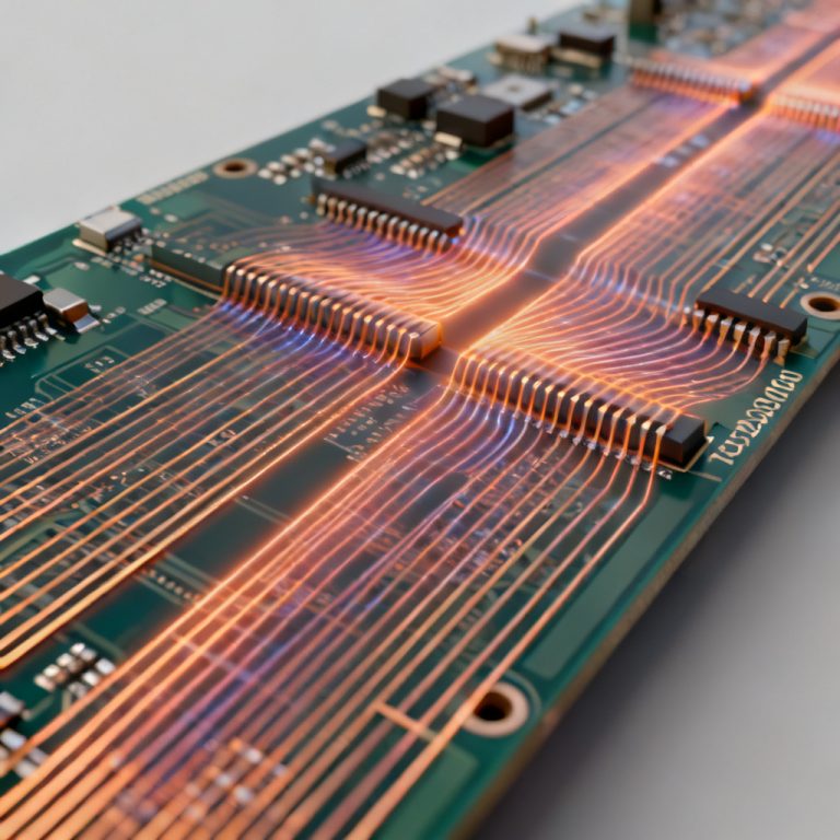
High-Speed Layout & 100Ω Differential Impedance Rules
High-speed differential pair routing is the core of optical module PCB design, directly determining signal integrity and bit error performance. The industry unified standard adopts 100Ω differential impedance for all optical module high-speed interfaces. The foundational rules for Differential Pair Routing apply directly to optical module layout. For complete impedance formulas and tolerance guidelines, refer to Impedance Matching.
| Design Parameter | Technical Requirement |
|---|---|
| Differential Impedance | 100Ω ±10% tolerance |
| Intra-Pair Length Skew | ≤2–3mil for 25G+; ≤2mil for 56G/100G PAM4 |
| Inter-Pair Length Matching | ±5mil overall deviation |
| Differential Pair Isolation Spacing | ≥4W (W = single trace width) |
| Max Vias Per Lane | ≤2 vias per high-speed channel |
| Back Drilling | Mandatory for 25G and above |
To reduce electromagnetic crosstalk, independent differential lanes must maintain enough isolation distance and avoid long parallel routing. Excessive vias cause impedance mutation and stub resonance. For 25G, 50G and 100G high-speed links, back drilling is strongly recommended to remove redundant via stubs, effectively reducing high-frequency insertion loss and improving eye diagram performance. Successful optical module PCB design depends on strict adherence to these impedance and routing rules.
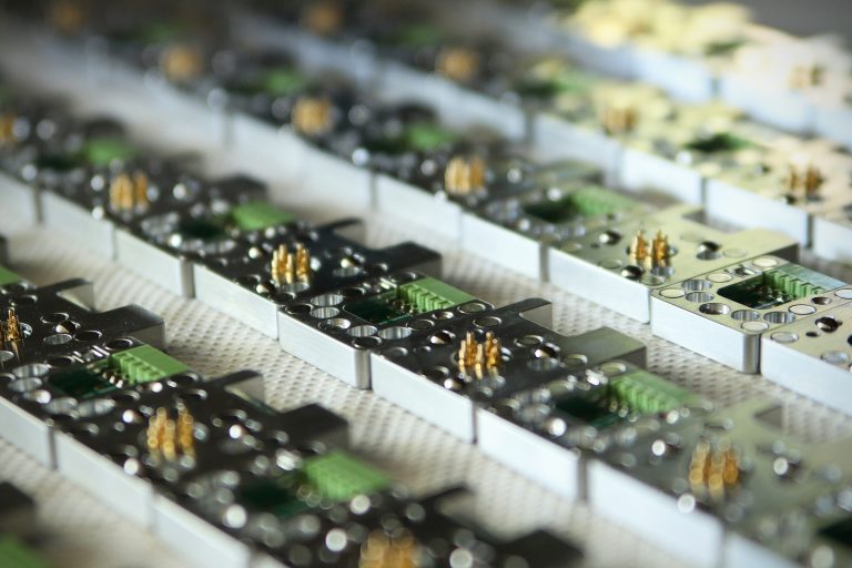
Optical Module Connector Layout Optimization
The connector area is the most vulnerable point of impedance discontinuity and signal reflection. Optimized layout can smooth signal transition and maintain stable reference return path. Every optical module PCB design should include these connector area optimizations.
Key Optimization Measures:
- Pad Size & Solder Mask Optimization: Adjust connector pad radius and solder mask opening to avoid sudden impedance change.
- Reference Plane Hollowing: Properly etch and hollow the ground/reference plane under the connector to compensate parasitic capacitance.
- Ground Return Via Arrangement: Place dense ground return vias closely beside signal vias, shorten high-frequency current return loop.
- Strict Differential Symmetry: Keep fully symmetric routing, trace width and spacing from transceiver chip to module connector.
This optimization method is widely adopted in TI and Intel official interface design guidelines, suitable for SFP/QSFP/OSFP connector mass-production layout.
Power Decoupling and Power Integrity Design
Optical modules feature high working current and strict power noise suppression requirements. Poor power design easily leads to voltage ripple, link instability and intermittent disconnection. Power integrity is often overlooked in optical module PCB design, but it directly impacts link stability and long-term reliability.
- High Current Design: Use thickened PCB copper layer and dense power via arrays to reduce DC resistance.
- Hierarchical Decoupling Configuration: Place low-ESR bulk capacitor and high-frequency 0402 ceramic capacitor near module power pins.
- Complete Ground Plane: Keep intact ground reference plane in power supply area to provide stable return path.
Thermal Management for Compact Optical Module PCB
Miniaturized high-density optical modules concentrate heat generation, and long-term high temperature will accelerate component aging and trigger overheating protection. Effective optical module PCB design must balance electrical performance with thermal dissipation requirements.
- Thermal Via Arrays: Arrange under high-heat chips and connector areas to conduct internal heat to outer copper layers.
- Thermal Conductive Pads: Match between optical module shell and PCB to transfer heat to system chassis.
- Increased Copper Thickness: Appropriately increase PCB copper thickness to improve heat conduction efficiency.
PCB Material Selection by Data Rate
PCB substrate Dk/Df loss directly determines high-speed signal attenuation. Designers must select materials according to single-channel rate to balance performance and cost. For detailed Dk/Df values of common laminates, refer to High-Speed PCB Material. Material selection is a critical decision in optical module PCB design that directly affects signal integrity and cost.
。10G–25G。25G–56G。56G–112G
| Data Rate | Recommended PCB Material Grade |
|---|---|
| ≤10G | Standard FR4 / Medium loss substrate |
| Low-loss substrate (Megtron 6, I-Speed) | |
| Optional low-loss or ultra-low-loss material | |
| Ultra-low-loss substrate (Megtron 8, Tachyon) |
Low-speed SFP+ can adopt conventional FR4 to control cost; 25G–56G QSFP28/QSFP56 needs low-loss material to control insertion loss; 56G–112G PAM4 high-rate OSFP/QSFP-DD must use ultra-low-loss substrate to ensure long-distance transmission performance.
Optical Module PCB Layout Checklist
Use this checklist for design review before PCB release. This checklist ensures your optical module PCB design meets all critical requirements before fabrication.
| ✅ | Item |
|---|---|
| ✅ | All high-speed differential pairs follow 100Ω ±10% impedance control |
| ✅ | Intra-pair skew controlled within 2–3mil (25G+) |
| ✅ | Differential pair spacing ≥4W for crosstalk isolation |
| ✅ | Connector reference plane hollowing and ground return vias completed |
| ✅ | Less than 2 vias per high-speed lane; 25G+ design adopts back drilling |
| ✅ | Hierarchical decoupling capacitors placed close to power pins |
| ✅ | Thermal via array arranged for heat dissipation |
Key Takeaways for Optical module PCB design
- Optical module PCB design is a systematic project integrating signal integrity, power integrity, layout optimization, material selection and thermal management.
- SFP, QSFP, QSFP-DD and OSFP have clear rate and bandwidth boundaries, which should be matched with corresponding impedance rules, routing constraints and substrate levels.
- The connector nearby area is the key bottleneck affecting signal quality; pad optimization, reference plane hollowing and return via layout must be strictly implemented.
- Material selection must be graded by speed: the higher the symbol rate and PAM4 modulation, the higher requirement for low-loss substrate.
- Power decoupling and thermal design determine long-term reliability of optical module equipment in data center and telecom scenarios.
- Following standard rules and checklist review can effectively avoid design iteration and mass production quality problems.
For a complete understanding of all high-speed interface layout requirements, return to the High-Speed Interfaces master page.
FAQ About Optical Module PCB Design
Q1: What is the standard differential impedance for optical module PCB?
Industry unified standard is 100Ω ±10% differential impedance for SFP, QSFP, QSFP-DD and OSFP high-speed lanes. This is the foundation of optical module PCB design.
Q2: How much length skew is allowed for 25G and above optical signals?
Intra-pair length skew ≤2–3mil for 25G NRZ; strictly controlled within ≤2mil for 56G/100G PAM4 signals.
Q3: Do all 25G+ optical module PCB need back drilling?
Yes, back drilling is strongly recommended to eliminate via stub resonance and reduce high-frequency signal loss.
Q4: Which PCB material is suitable for 400G/800G OSFP modules?
56G–112G PAM4 lanes require ultra-low-loss substrate like Megtron 8 or Tachyon series.
Q5: Why need reference plane hollowing under optical module connector?
To compensate parasitic capacitance of dense connector pins, balance impedance and reduce signal reflection.
Professional Optical Module PCB Design Support & Quote
If you are designing data center switch boards, telecom transmission equipment, enterprise network hardware or custom high-speed backplanes, you may need reliable optical module PCB design technical support.
Our team has rich engineering experience in SFP, QSFP, QSFP-DD and OSFP high-speed PCB layout, impedance simulation, layer stackup design, connector optimization, material selection and thermal design consultation. We support 10G/40G/100G mainstream modules and 400G/800G next-generation high-rate optical module one-stop design service.
© 2026 HighSpeedPCBs