Abstract
High-speed PCB mass production is the final stage of hardware development, where validated designs transition to volume manufacturing. For quantities of 500 to 50,000+ pieces, the focus shifts from design verification to batch consistency, high yield, process control, and cost optimization.
This pillar guide integrates three authoritative sources:
- PCBCart – Cost structure, BOM optimization, COPQ analysis
- JLCPCB – Panelization strategies, V-scoring, tab routing, DFM rules
- NextPCB – Prototype-to-production transition, AQL sampling, ICT vs flying probe
The result is a complete, engineer-approved reference for high-speed PCB mass production – suitable for hardware developers, procurement buyers, and industrial project managers.
Mass Production – Consistent Quality at Scale
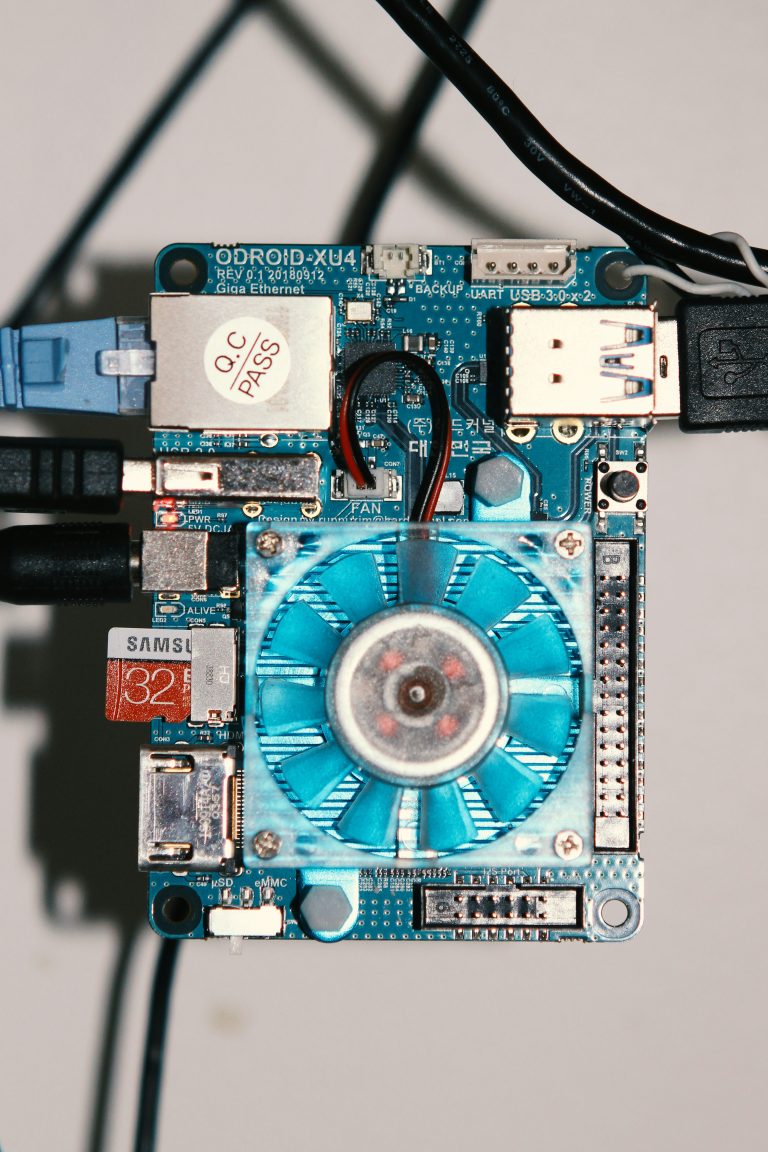
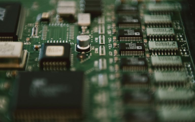
High speed PCB mass production represents the transition from design validation to volume deployment. After a design proves successful in prototype and pilot runs, high speed PCB mass production delivers consistent, repeatable, and cost-effective boards for commercial release. Typical quantities range from 500 to 50,000+ pieces. As part of our high-speed PCB prototyping service ecosystem, mass production is the natural final stage after successful pilot runs.
The primary goals of high-speed PCB mass production are: batch consistency – every batch performs identically; high yield – minimize defects (1% defect in 50,000 pieces = 500 scrap boards); process stability – SPC monitoring of critical steps; cost optimization – lowest per-unit pricing through volume; supply reliability – on-time delivery for production schedules.
For projects still in validation, consider our small batch PCB production service for 10–250 piece pilot runs before committing to high speed PCB mass production.
Mass Production Technical Capabilities
For detailed manufacturing capabilities, refer to PCB Manufacturing. For material data, see High-Speed PCB Material. High-speed PCB mass production supports 4–32 layers with mature processes.
| Parameter | Mass Production Capability |
|---|---|
| Layer Count | 4–32 layers (stable volume production) |
| Board Materials | FR4, High-speed laminates, Hybrid stackups |
| Impedance Control | ±10% standard (batch consistency guaranteed) |
| Special Processes | Backdrilling, HDI, Sequential lamination (mature) |
| Surface Finish | ENIG, HASL-LF, OSP, ENEPIG, Immersion Silver |
| Testing | AOI, Flying probe, TDR, X-ray, Four-wire Kelvin |
Volume Tiers and Pricing Structure
For impedance requirements, refer to Impedance Matching. The pricing below applies to high speed PCB mass production orders.
| Volume Tier | Engineering Fee | Unit Price Trend | Best For |
|---|---|---|---|
| 500–1,000 pcs | Low | Significant drop | First mass production run |
| 1,000–5,000 pcs | Very low | Stable | Sustained volume orders |
| 5,000–20,000 pcs | Minimal | Optimal | Large-scale deployment |
| 20,000+ pcs | Zero (re-order) | Locked best rate | Long-term recurring projects |
Cost Structure & Optimization Strategies
Understanding cost structure is essential for effective high speed PCB mass production planning. Volume PCB manufacturing achieves significant cost savings through scale.
| Cost Category | Typical Share | Optimization Strategy |
|---|---|---|
| BOM Components | 60–70% | Standardize values, use common packages |
| PCB Fabrication | 15–25% | Reduce layer count, optimize panelization |
| Assembly & Testing | 10–15% | SMT vs THT trade-off, ICT for high volume |
Layer count impact: 4-layer → 6-layer increases cost by approximately 40%. Odd layer counts cost 15% more than even layers. BOM standardization: Replace 10kΩ and 10.2kΩ resistors with common 10kΩ; use standardized component sizes (0402, 0603, 0805). These strategies directly benefit your high-speed PCB mass production budget.
COST VS QUALITY: A 1% defect rate in a 50,000-piece order = 500 defective boards – direct material waste plus rework cost. For volume PCB manufacturing, quality control is as important as cost control.
Panelization Strategies for High Efficiency
Panelization is essential for high speed PCB mass production. SMT equipment is designed for standard-sized panels, not individual small PCBs.
| Method | Best For | Advantages | Limitations |
|---|---|---|---|
| V-Cut (V-Scoring) | Straight-line rectangular boards | Lowest cost, fast depaneling | Straight lines only |
| Tab Routing (Mouse Bites) | Irregular shapes, multiple designs | Handles any shape | Requires manual depaneling |
| Breakaway Rails | Thin or flexible boards | Adds structural support | Extra material waste |
DFM rules: Component to V-cut ≥1.0mm; to tab edge ≥0.5mm; routing tab width 1.6–2.4mm; panel edge clearance 5mm minimum; tooling holes: 3 recommended; fiducial marks: 3 recommended. Panelization efficiency: Single-panel: 40–50% utilization; optimized panelization: 80–95% utilization – a key advantage of high-speed PCB mass production.
Quality Control & Testing Systems
Proper Return Path design validation is included in first article testing for high speed PCB mass production orders.
| Control Point | Method | Purpose |
|---|---|---|
| IQC | Raw material inspection | Verify laminate Tg, Dk/Df, copper thickness |
| SPC | Real-time monitoring | Detect drift in etching, lamination, drilling |
| First Article | Full test of first panel | Validate process setup |
| TDR | Sampling per batch | Verify impedance consistency |
| Electrical Test | Flying probe or ICT | 100% continuity and isolation |
ICT vs Flying Probe: Flying probe has no fixture cost but takes minutes per board. ICT has fixture cost ($2,000–5,000) but tests in seconds. Conversion threshold: 500–1,000 pieces – a critical decision point for high speed PCB mass production planning. AQL sampling per IPC-A-600: Class 1 (general) – standard AQL; Class 2 (dedicated) – tight AQL; Class 3 (medical/aerospace) – 100% inspection or zero-defect AQL.
Pilot Run to Mass Production Transition
High speed PCB mass production requires careful transition from pilot runs. Four key steps: 1. Evaluate pilot run results – Review yield rates, TDR reports; 2. Deep communication with supplier – Confirm process parameters; 3. DFM optimization – Apply lessons learned; 4. Establish quality system – Define AQL levels, sampling plans.
Skipping the pilot run and moving directly from prototype to high-speed PCB mass production is a common mistake that leads to yield issues and costly rework. A structured transition ensures stable, repeatable quality at scale for your volume PCB manufacturing project.
DFM Optimization & Best Practices
High speed PCB mass production benefits greatly from DFM optimization. Design simplification: Reduce layer count when possible (4-layer vs 6-layer saves 40%); maintain minimum trace width ≥0.1mm (4mil); use symmetrical stackup; avoid blind/buried vias unless necessary. These DFM rules reduce cost.
Component selection: Prefer standard values and common packages (0402, 0603, 0805); avoid EOL components; use manufacturer’s inventory parts.
Assembly optimization: SMD components only for fully automated assembly; THT requires manual insertion – higher cost. For volume PCB manufacturing, SMD is strongly preferred.
Complete Mass Production Checklist
Use this checklist before releasing your design to high speed PCB mass production:
| ✅ | Item |
|---|---|
| ✅ | Gerber RS-274X format (all layers) |
| ✅ | Drill files and IPC netlist |
| ✅ | BOM with manufacturer part numbers |
| ✅ | Material type, layer count, stackup confirmed |
| ✅ | Impedance requirements and tolerance specified |
| ✅ | Panelization method selected |
| ✅ | IPC Class (2 or 3) and AQL plan defined |
| ✅ | Golden sample reference established |
| ✅ | Quantity and lead time confirmed |
Key Takeaways for High Speed PCB Mass Production
- High speed PCB mass production (500–50,000+ pieces) focuses on batch consistency, high yield, and cost optimization
- Cost structure: BOM (60–70%), PCB fabrication (15–25%), assembly/testing (10–15%) – key to profitable volume PCB manufacturing
- Panelization improves material utilization from 40–50% to 80–95%
- Test strategy should convert from flying probe to ICT fixture at 500–1,000 pieces
- AQL sampling per IPC-A-600 matches product class (Class 3 = zero functional defects)
- Pilot run before mass production is mandatory – never skip this phase
- For cost-sensitive projects, consider copper thickness optimization
Frequently Asked Questions (FAQ)
Q1: What is the typical quantity range for high-speed PCB mass production?
High speed PCB mass production typically covers 500 to 50,000+ pieces, with flexible options for ongoing replenishment.
Q2: How does pricing change as volume increases?
Unit cost drops 30–40% from 500 to 5,000 pieces. Re-orders waive engineering fees entirely – a major advantage of high speed PCB mass production.
Q3: Why is panelization important for mass production?
Panelization improves material utilization from 40–50% to 80–95% and reduces handling time per board, directly lowering cost in high speed PCB mass production.
Q4: What is the difference between flying probe and ICT test?
Flying probe has no fixture cost but takes minutes per board. ICT has fixture cost ($2,000–5,000) but tests in seconds. Conversion threshold is 500–1,000 pieces for optimal volume PCB manufacturing.
Q5: What is AQL and how does it apply?
AQL is a sampling standard per IPC-A-600. Class 1 allows minor cosmetic defects; Class 3 requires zero functional defects – essential for medical and aerospace high speed PCB mass production.
Q6: Why do I need a golden sample?
A golden sample is the approved first-article board. It serves as the absolute reference for quality acceptance – any dispute is settled by comparing to the golden sample, protecting your high speed PCB mass production investment.
Q7: What certifications should a mass production supplier have?
ISO 9001 is minimum. IATF 16949 for automotive, ISO 13485 for medical, UL for safety, and RoHS/REACH for environmental compliance – all critical for high speed PCB mass production partners.
Get Your High Speed PCB Mass Production Quote
Ready to scale your validated design to volume production? Our high speed PCB mass production service supports 500 to 50,000+ pieces with consistent quality, process control, and global delivery.
What we offer: 4–32 layer PCBs with full material traceability; Impedance control: ±10% standard with batch consistency; Backdrilling, HDI, and hybrid stackup capabilities; Systematic quality control: IQC, SPC, first article, TDR sampling; ICT fixture testing for high-volume orders; Panelization optimization for 80–95% utilization; Simplified re-orders with waived engineering fees; ISO 9001 certified, IPC Class 2/3 compliant.
📧 Send your Gerber files, quantity target (500+ pieces), and volume forecast – we will provide free DFM review, panelization optimization, and competitive high speed PCB mass production quotation within 24 hours.
© 2026 HighSpeedPCBs