Master the calculation of 50Ω characteristic impedance for microstrip traces. Learn the exact formulas, key parameters (trace width, dielectric height, copper thickness), and practical PCB design rules for high-speed digital and RF applications. This guide is your definitive resource for achieving precise 50Ω characteristic impedance in microstrip designs.
Understanding 50Ω Characteristic Impedance in Microstrip Traces
In high-speed PCB design, maintaining a consistent 50Ω characteristic impedance for microstrip traces is critical to minimize signal reflections, ensure power transfer, and preserve signal integrity. Whether you are designing for RF circuits, high-speed digital interfaces (e.g., DDR, PCIe, USB 3.0), or microwave applications, the microstrip is one of the most common transmission line structures. This pillar content will guide you through the precise calculation methods, the influence of key PCB parameters, and practical considerations for manufacturing.
What is a Microstrip Transmission Line?
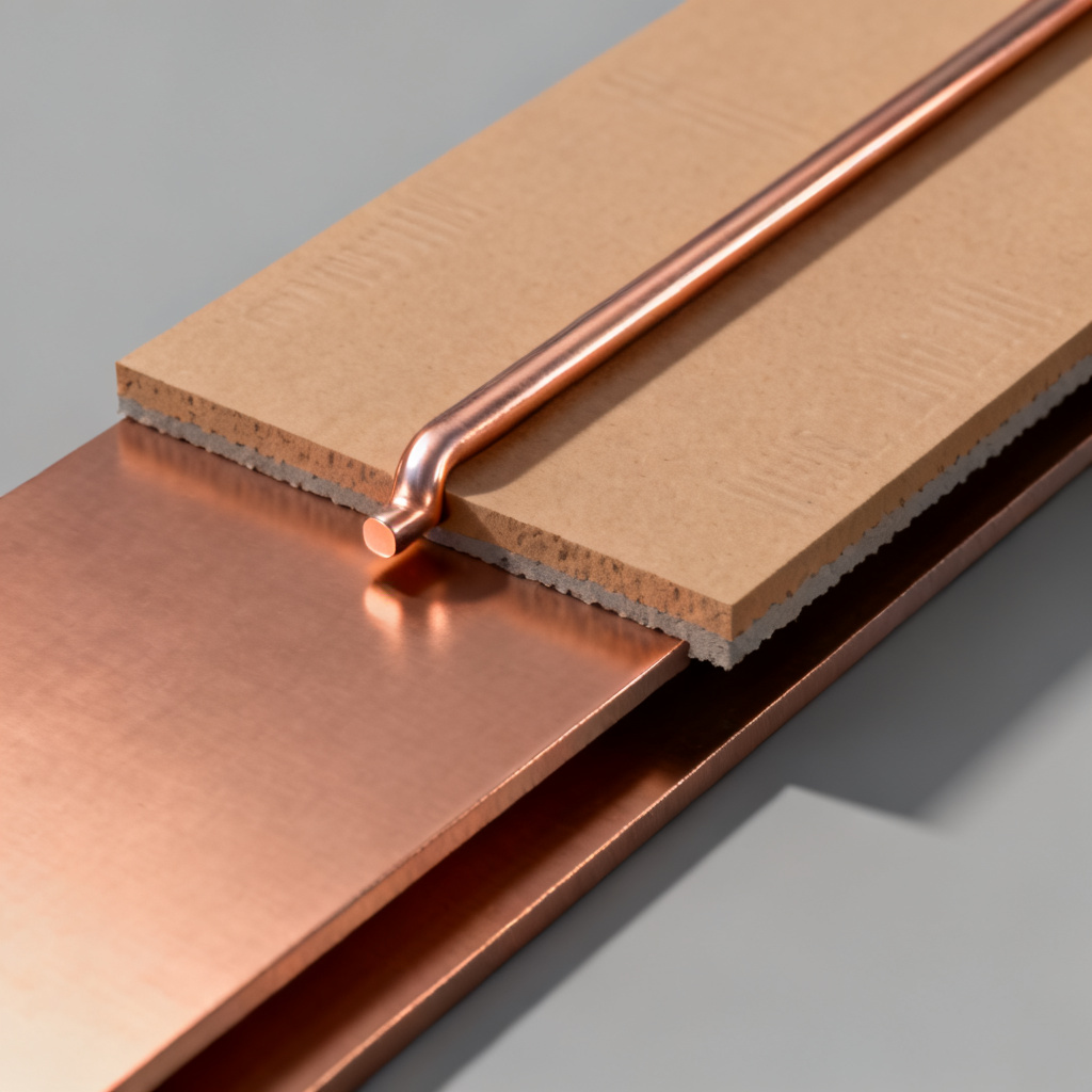
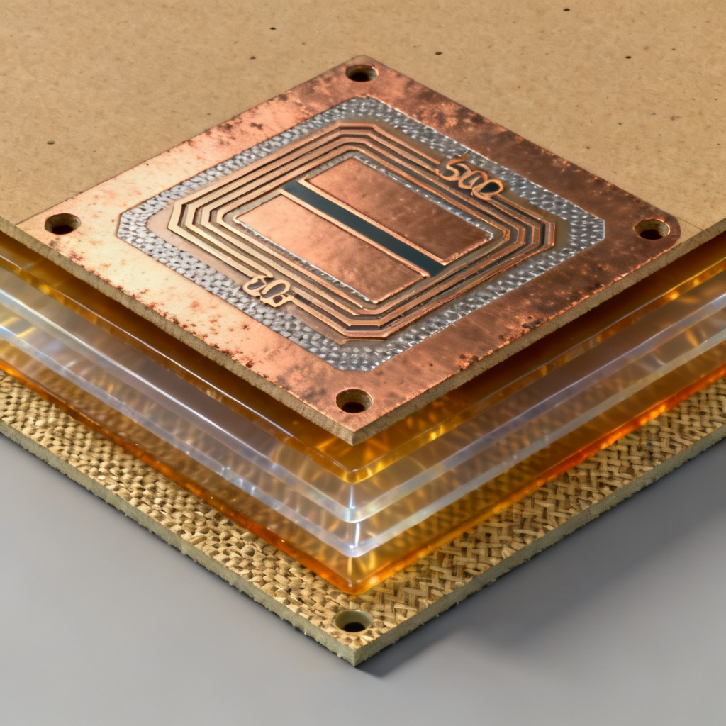
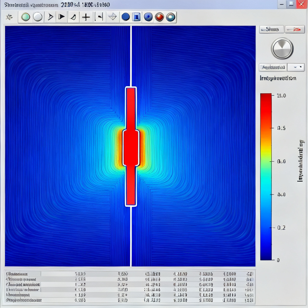
A microstrip transmission line consists of a conductive trace of width (W) on the top layer of a PCB, separated from a solid reference ground plane (typically on the next layer) by a dielectric material of thickness (H). The trace is exposed to air on top and the dielectric material below. Because the electric fields exist in both air (εr ≈ 1) and the PCB substrate (εr = 1 to 10), the effective dielectric constant (εeff) is a critical intermediate value used in 50Ω characteristic impedance calculations.
Key Formulas for 50Ω Characteristic Impedance Calculation
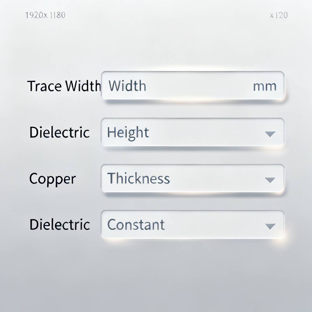
The characteristic impedance (Z0) of a microstrip trace depends on four primary physical parameters: trace width (W), dielectric height (H), copper thickness (T), and relative permittivity (εr) of the substrate material. There are two widely accepted formulas for calculating Z0: the IPC-2141A (Wheeler) approximation and the Schneider (Hammerstad & Jensen) model. Both yield similar results for typical PCB geometries.
Formula 1: IPC-2141A (Wheeler) Approximation
This formula is simple and suitable for initial estimates when T is negligible or accounted for separately.
Z0 = 87 / sqrt(εr + 1.41) * ln(5.98H / (0.8W + T))
Where H, W, and T are in the same units (e.g., mils). This formula works best when W/H is between 0.1 and 3.0.
Formula 2: Hammerstad & Jensen (Schneider) Model
This is more accurate for modern PCB designs and explicitly calculates the effective dielectric constant (εeff). First, calculate εeff:
εeff = (εr + 1)/2 + (εr - 1)/2 * (1 + 12H/W)^(-0.5)
Then, calculate Z0 for W/H ≤ 1:
Z0 = 60 / sqrt(εeff) * ln(8H/W + W/4H)
For wider traces (W/H > 1):
Z0 = 120π / (sqrt(εeff) * (W/H + 1.393 + 0.667 * ln(W/H + 1.444)))
Step-by-Step Calculation Example for 50Ω on FR4
Let’s calculate the required trace width for a standard 4-layer FR4 stackup: Core thickness = 10 mils (H), 1 oz copper (T = 1.4 mils), εr = 4.5.
- Estimate W using IPC-2141A: Set Z0 = 50, solve for W. A common starting point is W ≈ 1.8 * H. For H=10 mils, W ≈ 18 mils.
- Refine using Hammerstad & Jensen: Weff = W + 1.5*T = 18 + 2.1 = 20.1 mils. W/H = 20.1/10 = 2.01 (use wide trace formula). εeff = (4.5+1)/2 + (4.5-1)/2 * (1 + 12*10/20.1)^(-0.5) = 2.75 + 1.75 * 0.378 = 3.41. Z0 = 120π / (√3.41 * [2.01 + 1.393 + 0.667*ln(2.01+1.444)]) = 120π / (1.847 * 4.23) = 376.99 / 7.81 = 48.3Ω.
- Iterate: To get exactly 50Ω, slightly reduce W. After a few iterations, a trace width of ~17.5 mils (with Weff = 19.6 mils, W/H=1.96) yields Z0 ≈ 50.1Ω.
Key Parameters That Influence 50Ω Characteristic Impedance
Understanding how each parameter affects 50Ω characteristic impedance is essential for precise design.
| Parameter | Effect on 50Ω Characteristic Impedance |
|---|---|
| Dielectric Height (H) | Increasing H raises impedance. For 50Ω, H is the most sensitive parameter. A 1-mil change in H can shift Z0 by 2-3Ω. |
| Trace Width (W) | Wider traces lower impedance. For 50Ω, W is typically 1.5 to 2.5 times H for standard FR4. |
| Copper Thickness (T) | Thicker copper (e.g., 2 oz vs 1 oz) reduces impedance slightly (by 1-3Ω) because it increases the effective trace width. |
| Dielectric Constant (εr) | Higher εr lowers impedance. FR4’s εr varies with frequency (e.g., 4.5 at 1 GHz, 4.2 at 10 GHz). Use the value at your operating frequency for accuracy. |
| Solder Mask | Solder mask has a dielectric constant (~3.5-4.0) and can lower Z0 by 1-3Ω. For high-precision designs, account for solder mask thickness (typically 0.5-1 mil) over the trace. |
Practical Stackup Design Rules for 50Ω Microstrip
To achieve reliable 50Ω characteristic impedance, follow these design rules:
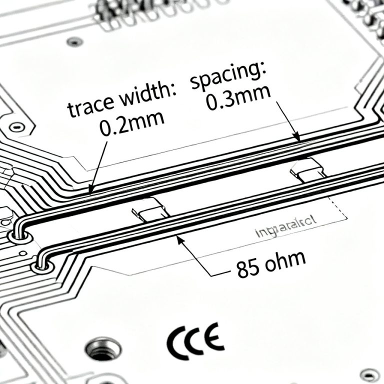
- Choose a Controlled Impedance Stackup: Work with your PCB manufacturer to specify a stackup that includes a defined dielectric height (H) between the signal layer and the reference plane. Standard prepreg thicknesses for 50Ω microstrip on FR4 are 4 mils, 6 mils, 8 mils, or 10 mils.
- Use a 2D Field Solver for Accuracy: The closed-form formulas above are excellent for estimation, but for production-level designs, use a 2D field solver (e.g., Polar Si9000, Simbeor, or Altium’s Impedance Calculator) that accounts for copper roughness, solder mask, and trapezoidal trace cross-sections.
- Maintain a Continuous Ground Plane: The reference plane must be solid and unbroken directly under the microstrip trace for the entire length. Avoid splitting the ground plane or routing over gaps.
- Keep Traces Away from Board Edges: Maintain a distance of at least 5x the trace width from the edge of the ground plane to avoid edge effects that alter impedance.
- Minimize Discontinuities: Avoid sharp 90-degree corners (use 45-degree chamfers or curved bends). Ensure via transitions have proper anti-pads and return vias to maintain impedance.
Why 50Ω is the Industry Standard
The 50Ω standard is a compromise between minimum attenuation (around 77Ω for air dielectric) and maximum power handling (around 30Ω for air dielectric). 50Ω offers a balanced trade-off for most RF and high-speed digital applications. It is also compatible with common test equipment (e.g., network analyzers, oscilloscopes with 50Ω inputs).
Common Mistakes to Avoid
When calculating 50Ω characteristic impedance, avoid these pitfalls:
- Using a Single Formula Without Verification: Different formulas give slightly different results. Always cross-check with a field solver.
- Ignoring Copper Thickness: For thick copper (2 oz or more), the trace’s sidewall contribution is significant. Use Weff in formulas.
- Assuming FR4’s εr is Constant: FR4’s dielectric constant varies with frequency and resin content. For high-speed designs (>1 GHz), specify a material with a stable εr (e.g., Rogers 4350B) or get a data sheet value from your laminate supplier.
- Neglecting Solder Mask: If you apply solder mask over the microstrip trace, the impedance will drop. For tight tolerances (±5%), include solder mask in your simulation.
Industry Terminology Explained
Characteristic impedance (Z0): The constant ratio of voltage to current in a transmission line without reflections. For microstrip, it is determined by geometry and material properties.
Effective dielectric constant (εeff): The weighted average of the dielectric constants of air and the PCB substrate, accounting for the field distribution.
Controlled impedance: A manufacturing process that ensures the impedance of a trace falls within a specified tolerance (e.g., ±5% or ±10%).
Field solver: A software tool that uses numerical methods (e.g., finite element analysis) to accurately compute impedance, accounting for real-world effects like copper roughness and solder mask.
Comparison: Our PCB Manufacturing vs. Standard Approaches
At [Your Company Name], we specialize in manufacturing high-speed PCBs with tight impedance tolerances (±5% or better). Unlike standard fabricators who may rely solely on closed-form formulas, we use advanced 2D field solvers and rigorous testing to guarantee 50Ω characteristic impedance across your entire board. Our controlled impedance stackup options include a wide range of dielectric heights and materials, ensuring your design meets both performance and budget requirements.
Frequently Asked Questions
How do I calculate 50Ω characteristic impedance for microstrip traces?
Use the IPC-2141A or Hammerstad & Jensen formulas with your trace width (W), dielectric height (H), copper thickness (T), and dielectric constant (εr). For production accuracy, always verify with a 2D field solver.
What is the standard tolerance for 50Ω characteristic impedance in PCB manufacturing?
Industry standard tolerance is ±10%, but many high-speed applications require ±5% or better. At [Your Company Name], we offer ±5% tolerance as standard for controlled impedance designs.
Does solder mask affect 50Ω characteristic impedance?
Yes, solder mask can lower impedance by 1-3Ω. For precise designs, include solder mask thickness and dielectric constant in your calculations or simulation.
Why is 50Ω the standard impedance for RF and high-speed digital?
50Ω offers an optimal balance between minimum signal attenuation (77Ω) and maximum power handling (30Ω), making it suitable for a wide range of applications and compatible with common test equipment.
“`