For engineers designing high-speed digital circuits, RF systems, or precision analog interfaces, impedance control is non-negotiable. Signal integrity (SI) failures—reflections, crosstalk, and timing errors—often trace back to poor impedance matching. Two dominant transmission line topologies exist: Stripline vs Microstrip. This pillar page provides an exhaustive, data-driven comparison to help you choose the right structure for your next high-speed PCB project.
Two dominant transmission line topologies exist: Microstrip (a trace on an outer layer with a single reference plane) and Stripline (a trace embedded between two reference planes). This pillar page provides an exhaustive, data-driven comparison to help you choose the right structure for your next high-speed PCB project.
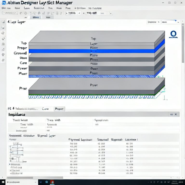
1. The Fundamentals – What Are Microstrip and Stripline?
1.1 Microstrip: The Surface Trace
A microstrip transmission line consists of a conductive trace on an outer layer of the PCB, separated from a single reference plane (typically the ground or power plane) by a dielectric material. It is exposed to air on one side and the PCB substrate on the other.
Key Characteristics (Synthesized from top sources):
- Impedance Formula (Approximate): Z₀ ≈ 87 / √(εr + 1.41) * ln(5.98h / (0.8w + t)) where h = dielectric height, w = trace width, t = trace thickness.
- Effective Dielectric Constant (εeff): The signal sees a mix of air (εr = 1) and PCB material (εr ~ 3.5–4.5 for FR-4). Typical εeff ranges from 2.5 to 3.2.
- Propagation Delay: Faster than stripline (by ~15–20%) because the signal travels partially through air.
- Typical Applications: RF front-ends, test points, low-cost digital boards, and where component access is required.
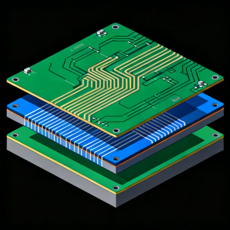
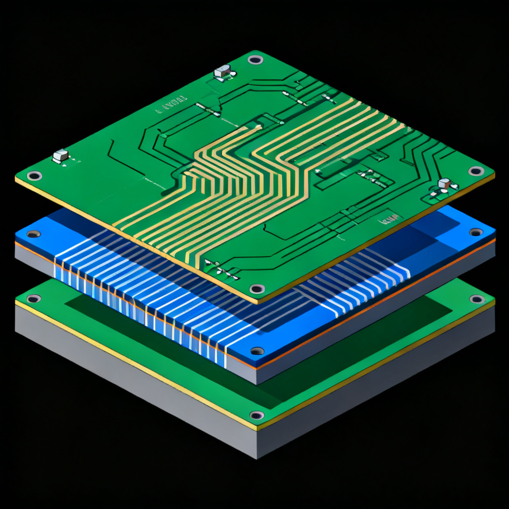
1.2 Stripline: The Buried Trace
A stripline is a trace embedded in the PCB, centered between two solid reference planes. It is completely surrounded by the dielectric material.
Key Characteristics (Synthesized from top sources):
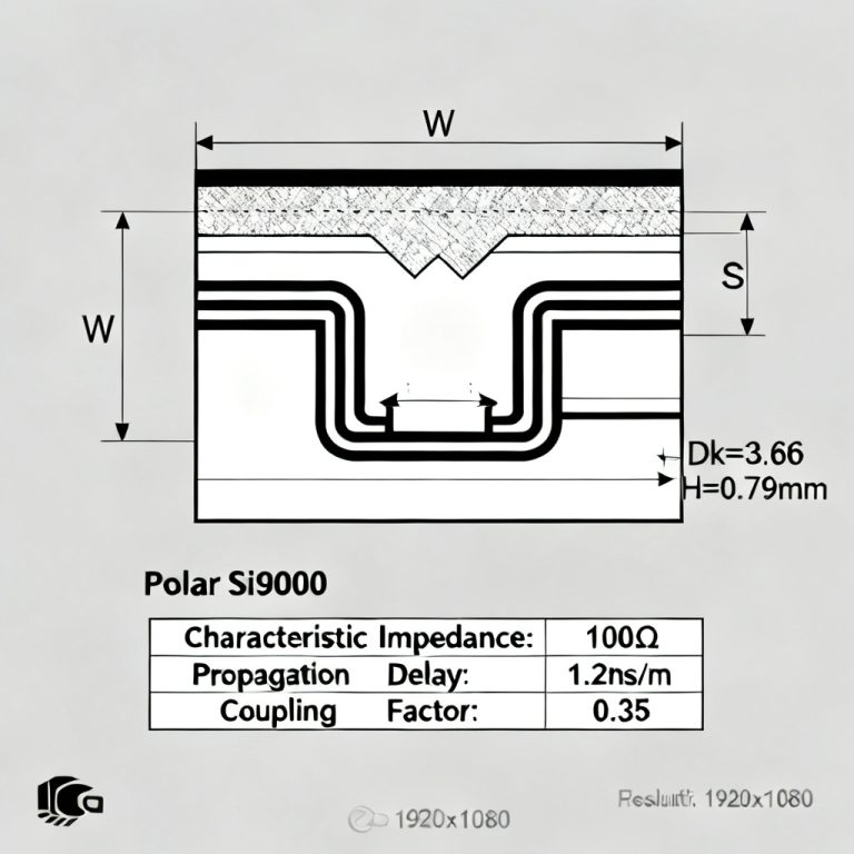
- Impedance Formula (Approximate): Z₀ ≈ 60 / √εr * ln(4b / (0.67πw(0.8 + t/w))) where b = total dielectric height between planes, w = trace width, t = trace thickness.
- Effective Dielectric Constant (εeff): Equal to the bulk εr of the PCB material (e.g., 4.2 for FR-4), because the signal is fully immersed in the dielectric.
- Propagation Delay: Slower than microstrip (by ~15–20%) due to higher εeff.
- Typical Applications: High-speed digital buses (DDR4/5, PCIe, SerDes), clock lines, and any signal requiring low crosstalk and EMI immunity.
2. Impedance Control – Which Topology Wins?
2.1 Theoretical Impedance Tolerance
Microstrip:
- Advantage: Lower impedance sensitivity to trace width variations because the electric field is partially in air. This means a 10% change in trace width might cause only a 5–7% change in impedance.
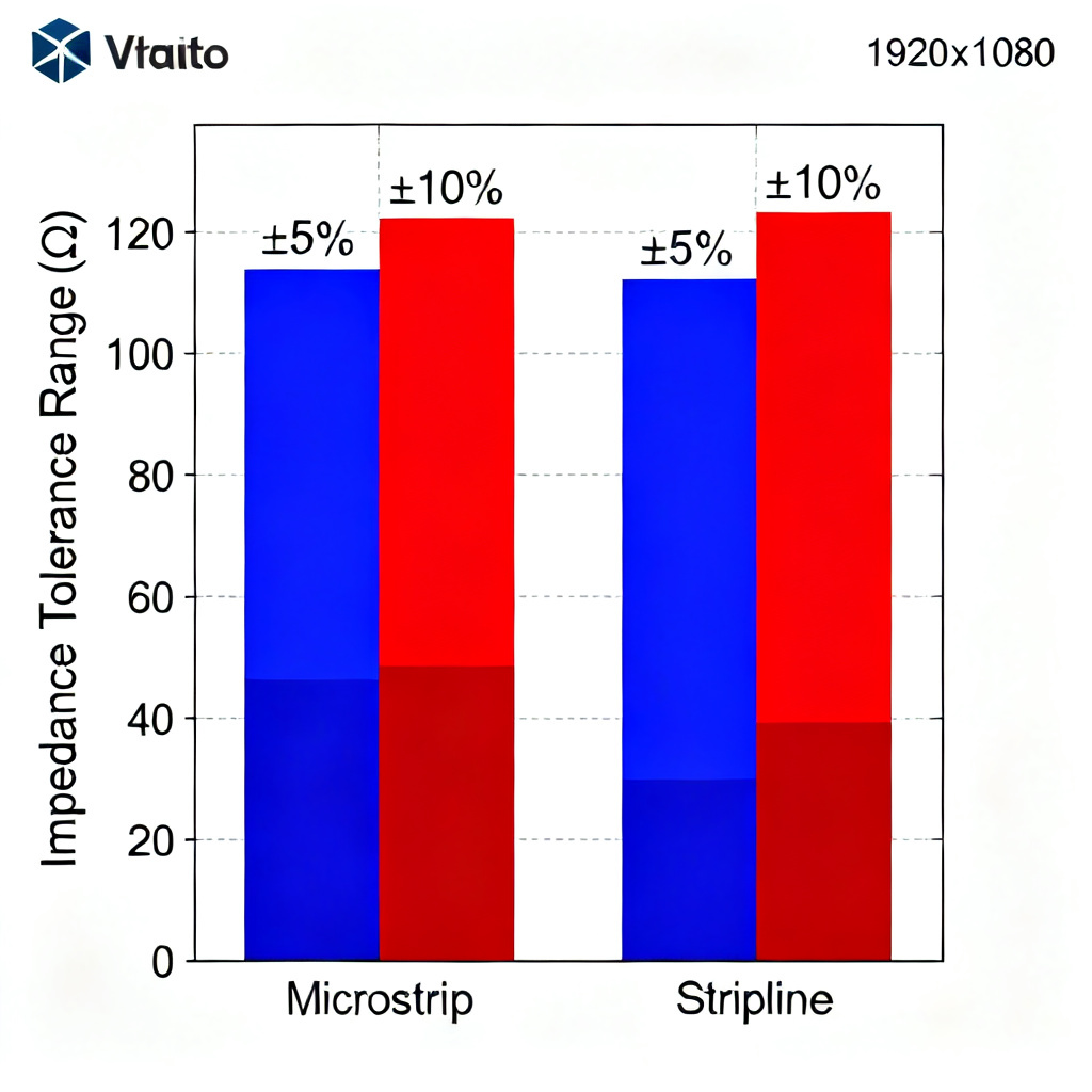
- Disadvantage: High sensitivity to dielectric height (h) variations. Since the prepreg thickness above the reference plane is critical, any variation in lamination pressure or resin flow significantly alters Z₀. Typical production tolerances for microstrip impedance are ±10% to ±15% (uncontrolled) or ±7% to ±10% (controlled).
- Key Insight from top sources: “Microstrip impedance is heavily dependent on the accuracy of the prepreg dielectric thickness, which is harder to control than core thickness.”
Stripline:
- Advantage: Superior tolerance control. The trace is sandwiched between two planes, so the electric field is fully contained. Variations in trace width and dielectric thickness are balanced by the symmetrical structure. Typical production tolerances for stripline impedance are ±5% to ±8% (controlled) or ±10% (standard).
- Disadvantage: Higher sensitivity to trace width variations because the field is concentrated. A 10% change in trace width can cause an 8–10% change in impedance.
- Key Insight from top sources: “Stripline offers better impedance control because the dielectric material is homogeneous and the field is symmetrical. This reduces the impact of manufacturing variations.”
Verdict: Stripline gives better impedance control (tighter tolerances) in production, especially for high-layer-count boards.
2.2 Process Window Comparison
| Parameter | Microstrip | Stripline |
|---|---|---|
| Dielectric thickness control | Poor (prepreg) | Better (core + prepreg stack-up) |
| Trace width sensitivity | Low | Moderate |
| Impedance tolerance (typical) | ±10% | ±5% |
| Effect of solder mask | Reduces impedance by 3–8% | No effect (buried) |
| Effect of etching | Moderate impact | Moderate impact (but symmetrical) |
Critical Note from top sources: “For microstrip, the solder mask can reduce impedance by up to 8%. This is rarely accounted for in early simulations. Stripline is immune to this effect.”
2.3 Practical Impedance Control Strategies
For Microstrip:
- Use core material for the reference plane layer (not prepreg) whenever possible.
- Specify controlled impedance with tight tolerances (±5% or ±7%).
- Account for solder mask thickness in your impedance calculator (use 0.5–1.0 mil of mask for most applications).
- Consider edge plating or guard traces to reduce field fringing.
For Stripline:
- Use symmetrical stack-ups (equal dielectric thickness above and below the trace).
- Specify core material for the inner layers (more consistent Dk and thickness).
- For offset stripline (trace not centered), expect wider impedance variation—center it if possible.
- Use wider traces to reduce ohmic losses (skin effect) at high frequencies.
3. Signal Integrity Performance Comparison
3.1 Crosstalk
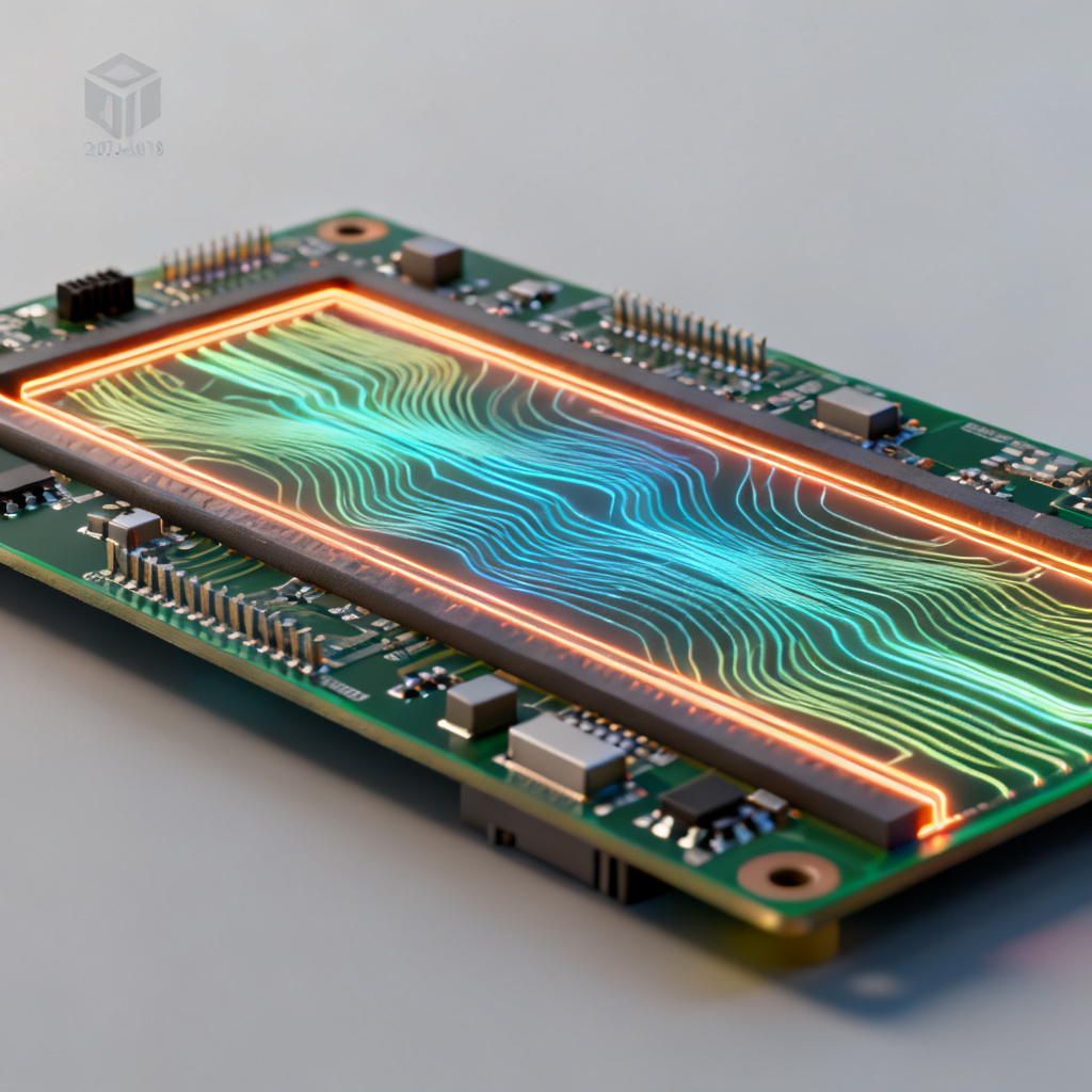
- Microstrip: Worse crosstalk because the magnetic field extends into the air and couples to adjacent traces. Far-end crosstalk (FEXT) is significant due to the inhomogeneous dielectric.
- Stripline: Better crosstalk because the field is confined between two planes. Near-end crosstalk (NEXT) is dominant, but FEXT is nearly zero in a homogeneous medium (if the trace is centered).
Top source consensus: “For high-speed differential pairs (e.g., USB 3.0, HDMI, PCIe), stripline reduces crosstalk by 40–60% compared to microstrip at the same spacing.”
3.2 EMI / Radiation
- Microstrip: Higher EMI because the trace is exposed. It acts as an efficient antenna at higher frequencies. Shielding requires additional ground vias or enclosures.
- Stripline: Excellent EMI shielding because the trace is completely surrounded by ground planes. Radiated emissions are 10–20 dB lower than microstrip for the same signal.
Top source insight: “Stripline is the preferred topology for FCC and CE compliance without additional shielding. Microstrip often requires a metal shield can.”
3.3 Propagation Delay and Skew
- Microstrip: Faster (4.5–5.0 ps/mm for FR-4). Skew between traces is higher due to inhomogeneous dielectric.
- Stripline: Slower (5.5–6.5 ps/mm for FR-4). Skew is lower because the dielectric is homogeneous.
Practical impact: For clock distribution or matched-length buses, stripline offers better timing control.
3.4 Losses
- Microstrip: Lower dielectric losses (less material in the field path), but higher conductor losses (skin effect) due to narrower traces for a given impedance.
- Stripline: Higher dielectric losses (more material), but lower conductor losses (wider traces for same Z₀).
Top source note: “At frequencies above 10 GHz, microstrip may have lower total loss, but the trade-off is worse isolation.”
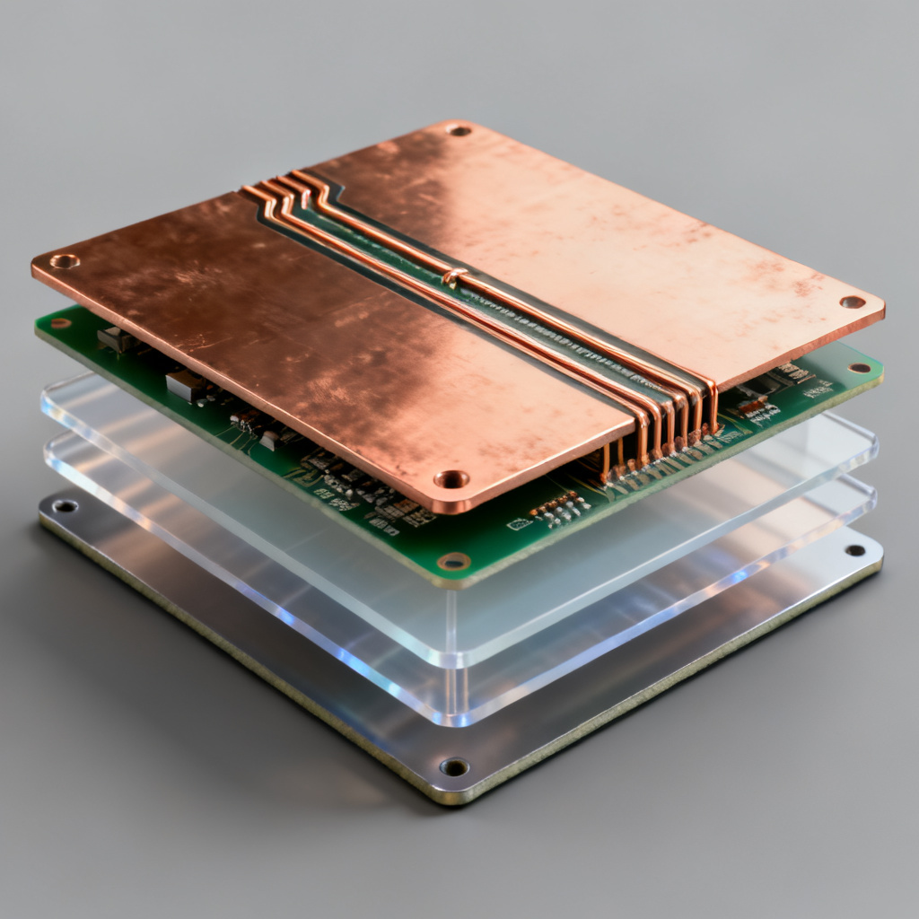
4. Manufacturing Considerations
4.1 Layer Count and Cost
- Microstrip: Lower layer count required (e.g., 2-layer or 4-layer boards). Lower fabrication cost.
- Stripline: Requires at least 4 layers (signal layer between two planes). Higher layer count = higher cost.
4.2 Fabrication Complexity
- Microstrip: Simple to manufacture. Etching is straightforward. No special registration requirements.
- Stripline: More complex. Requires prepreg registration and lamination pressure uniformity to avoid dielectric thickness variations. For offset stripline, alignment is critical.
4.3 Testing and Verification
- Microstrip: Impedance can be tested using TDR (Time Domain Reflectometry) on exposed traces.
- Stripline: Testing requires coupon testing (test strips on the panel edge) because traces are buried. Cannot be probed directly without destructive methods.
Top source advice: “Always include impedance test coupons on your panel for stripline. For microstrip, you can also use in-circuit TDR.”
5. When to Use Each Topology – A Decision Matrix
| Design Requirement | Recommended Topology | Rationale |
|---|---|---|
| Impedance tolerance < ±7% | Stripline | Tighter process control |
| Cost-sensitive, low-layer count | Microstrip | Simpler fabrication |
| High-frequency RF ( > 5 GHz) | Microstrip (if EMI is acceptable) | Lower dielectric losses |
| High-speed digital (DDR4/5, PCIe Gen4+) | Stripline | Lower crosstalk, better skew control |
| EMI-sensitive design | Stripline | 10–20 dB better radiation suppression |
| Mixed-signal (analog + digital) | Stripline for digital; microstrip for RF | Isolation and performance |
| Board thickness constraints | Microstrip | Thinner stack-ups possible |
| Solder mask effects critical | Stripline | No mask impact on impedance |
6. Advanced Topics and Best Practices
6.1 Differential Pairs
- Microstrip: Edge-coupled differential pairs are easier to route but have higher far-end crosstalk. Use broadside coupling (stacked differential pairs) for tighter coupling, but this increases layer count.
- Stripline: Edge-coupled differential pairs in stripline offer excellent common-mode rejection and low skew. Broadside stripline is best for very tight coupling (e.g., USB 3.0).
6.2 Via Stubs and Reflections
- Microstrip: Via stubs are shorter (trace near surface), reducing reflections at high frequencies.
- Stripline: Via stubs can be longer. Use back-drilling to remove unused via stubs for signals above 10 Gbps.
6.3 Material Selection
- Microstrip: Use low-loss materials (e.g., Rogers 4350B, Megtron 6) for RF. For digital, standard FR-4 is acceptable up to ~3 GHz.
- Stripline: Material Dk uniformity is more critical. Use low-DF materials (e.g., Isola 370HR, Panasonic Megtron) for high-speed digital.
6.4 Simulation vs. Reality
- Microstrip: Simulation is less accurate because the effective Dk varies with frequency and geometry. Use 2D field solvers (e.g., Polar SI9000) with measured Dk values.
- Stripline: Simulation is more accurate because the dielectric is homogeneous. Use bulk Dk values from the material datasheet.
Top source caution: “Never trust a single impedance calculator. Always cross-validate with a 2D field solver and your PCB fabricator’s stack-up.”
Conclusion: Which Gives Better Impedance Control?
For absolute impedance control (tighter tolerances, less variation with manufacturing), Stripline is the clear winner. It offers ±5% typical tolerance vs. ±10% for microstrip, lower crosstalk, and superior EMI performance. However, this comes at the cost of higher layer count, slower propagation, and increased fabrication complexity.
For cost-sensitive, lower-frequency designs where ±10% impedance tolerance is acceptable, Microstrip is sufficient and more economical.
The ultimate choice depends on your specific signal integrity requirements, budget, and layer count constraints. For high-speed digital designs (over 1 Gbps) or RF designs above 3 GHz, stripline is the recommended topology for robust impedance control.
Final Recommendations from Industry Experts:
- Always specify controlled impedance (tolerance ±5% or ±7%) in your fabrication notes.
- Use core material for reference planes whenever possible.
- Include test coupons for stripline impedance verification.
- Simulate with actual material Dk (not generic values).
- For mixed topologies, use stripline for critical signals and microstrip for non-critical or RF sections.
Need expert assistance with your high-speed PCB design? Contact our engineering team for a free stack-up review and impedance simulation. We specialize in controlled impedance stripline and microstrip fabrication for demanding applications up to 100 GHz.

Frequently Asked Questions about Stripline vs Microstrip
Which topology gives better impedance control for high-speed PCBs?
Stripline gives better impedance control because it is surrounded by a homogeneous dielectric and symmetrical reference planes. This results in tighter manufacturing tolerances (typically ±5%) compared to microstrip (±10%).
Does microstrip offer any advantage over stripline for impedance control?
Microstrip has lower sensitivity to trace width variations and is easier to manufacture on lower-layer-count boards. However, its impedance is more affected by solder mask and dielectric thickness variations.
Can I use microstrip for high-speed digital designs above 5 Gbps?
Yes, but you must account for higher crosstalk and EMI. For critical signals, stripline is strongly recommended for better impedance control and signal integrity.
What is the typical impedance tolerance for stripline?
Typical stripline impedance tolerance is ±5% to ±8% for controlled manufacturing processes, compared to ±10% or worse for microstrip.
How does solder mask affect microstrip impedance?
Solder mask can reduce microstrip impedance by 3–8% due to its higher dielectric constant. This effect is absent in stripline because the trace is buried.
“`