In high-speed PCB design, maintaining consistent impedance is critical for signal integrity, and tapered traces provide a gradual width transition to minimize impedance mismatch and reflections. This guide explains when and how to use them effectively.
In the world of high-speed digital and RF PCB design, maintaining consistent impedance is paramount. As signal frequencies rise into the GHz range, even minor discontinuities—like a sudden change in trace width—can cause reflections, signal degradation, and electromagnetic interference (EMI). This is where tapered traces become an indispensable tool.
A tapered trace is a gradual, linear transition from a wider trace width to a narrower one (or vice versa), designed to minimize impedance mismatch. Unlike abrupt width changes, which create a sharp impedance discontinuity that reflects signal energy back to the source, a taper provides a smooth, controlled transition. This article serves as your ultimate guide to understanding, designing, and manufacturing tapered traces for impedance-controlled PCBs, covering everything from fundamental theory to advanced application scenarios.
Understanding Impedance Control and Signal Integrity
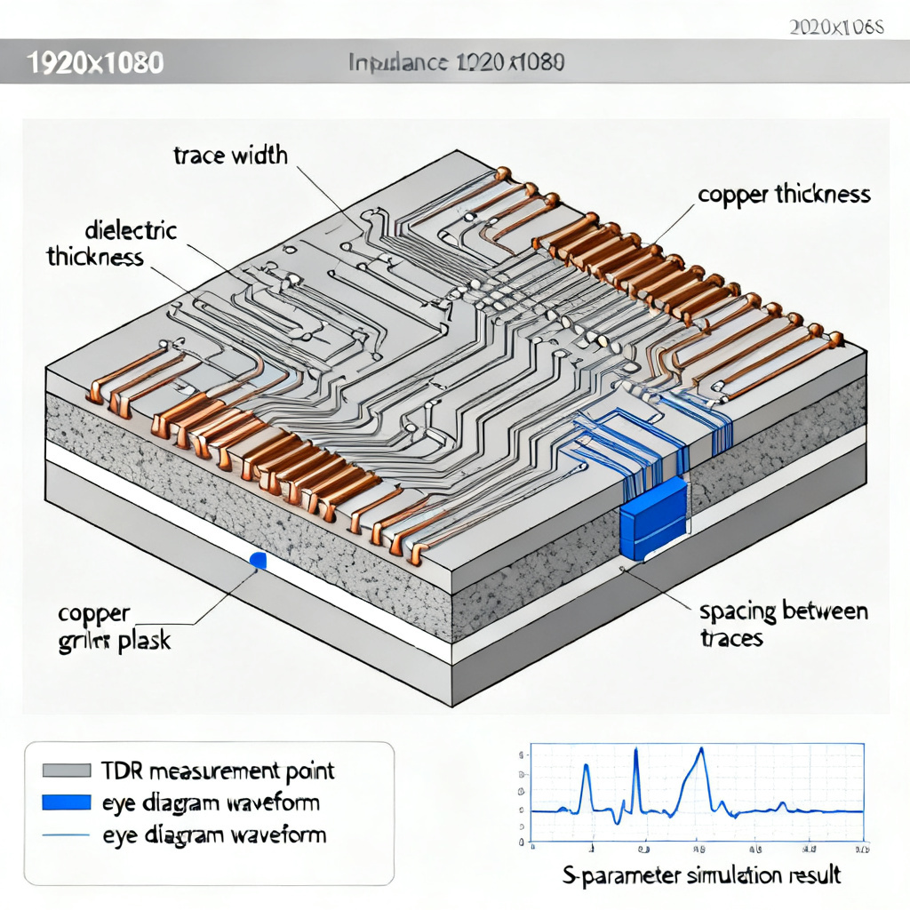
Before diving into tapered traces, it’s crucial to grasp the basics of impedance control. In high-speed PCB design, characteristic impedance (Z₀) is the constant impedance that a transmission line exhibits along its length. Common target values are 50Ω (single-ended) or 100Ω (differential). Maintaining this value is critical because any deviation causes partial signal reflection, leading to ringing, crosstalk, and timing errors.
Key factors that determine Z₀ include:
- Trace width (W) and thickness (T)
- Dielectric constant (Dk) and height (H) of the substrate
- Copper foil roughness
- Solder mask thickness
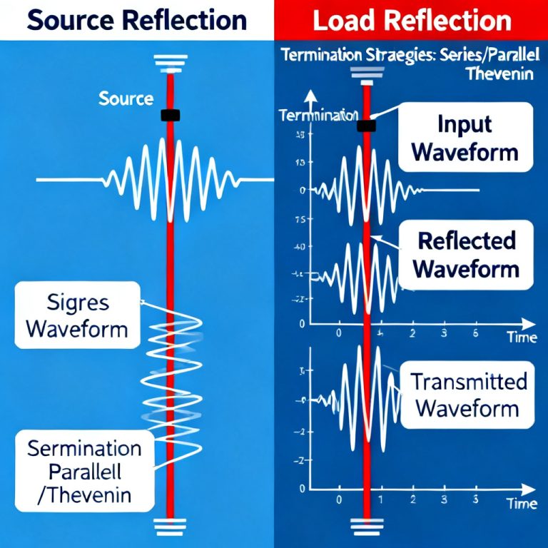
When you must change trace width—for instance, to connect a wide BGA pad to a narrow routing channel—an abrupt step creates a localized impedance spike or dip. This discontinuity acts like a small capacitor or inductor, degrading signal quality. A tapered trace solves this by gradually changing the width over a sufficient length, allowing the electromagnetic field to adapt smoothly, thereby preserving impedance continuity.
When to Use Tapered Traces: Key Scenarios
Tapered traces are not a universal solution; they are specifically required in certain high-speed and RF design contexts. Based on expert analysis, the following are the primary scenarios where tapering is essential:
Connecting to Component Pads (BGA, QFN, and Connectors)
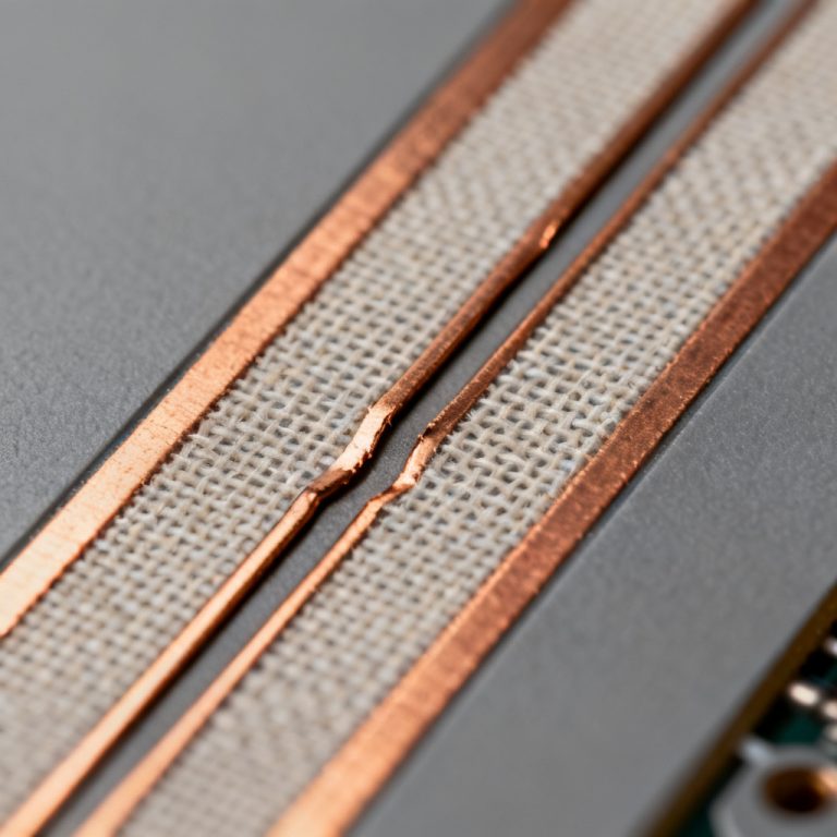
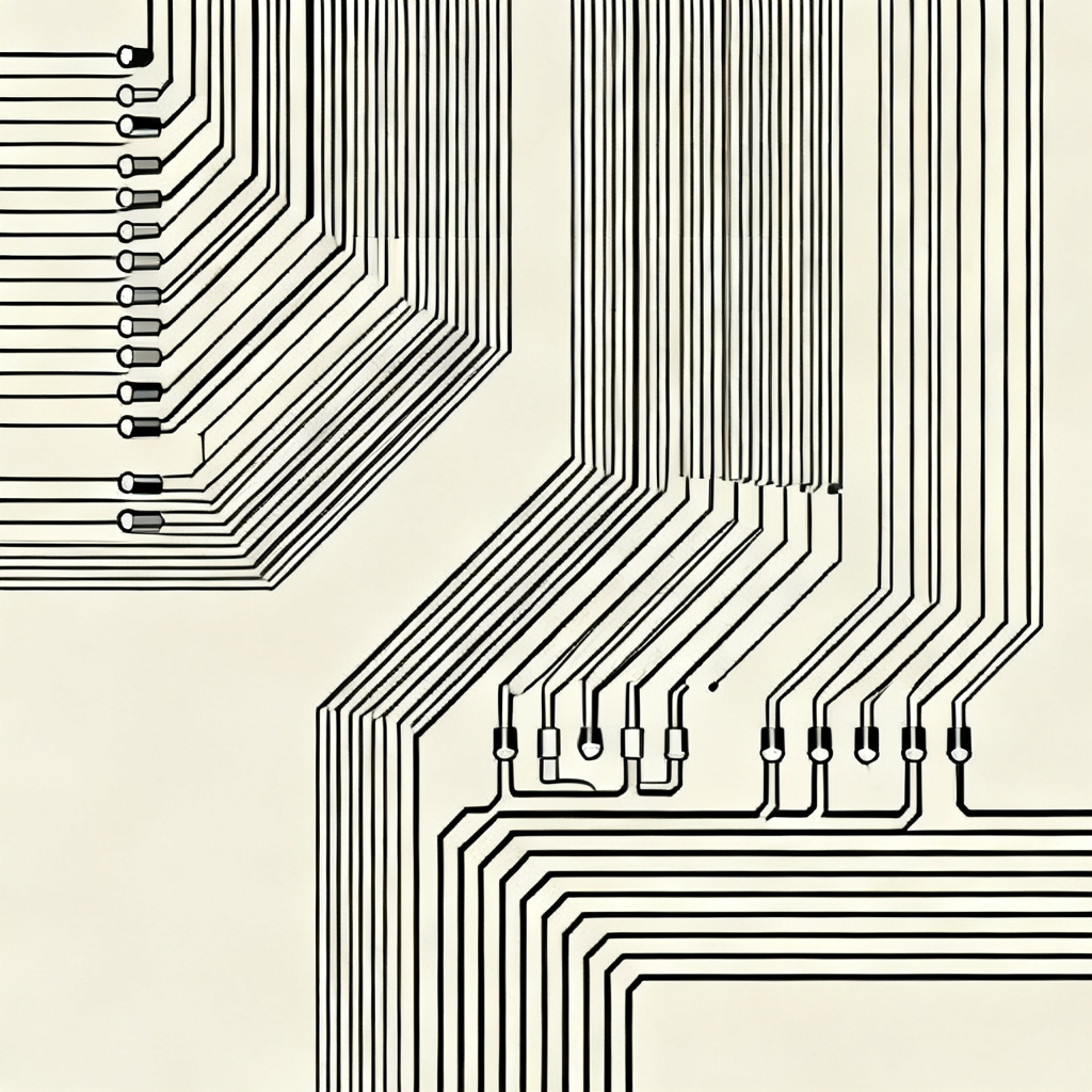
Modern high-pin-count components, such as BGAs with 0.5mm or 0.4mm pitch, have very small pads. The trace width required to escape from these pads (often 3-4 mils) is much narrower than the typical 50Ω trace width (e.g., 8-10 mils on a standard stackup). An abrupt transition from a 10-mil trace to a 4-mil pad would cause a severe impedance discontinuity. A tapered trace (often called a “dog-bone” or “fan-out” taper) smoothly widens from the pad to the target trace width over a short distance, minimizing reflection.
Routing Between Different Impedance Zones
In mixed-signal designs or RF front-ends, you may need to transition between different impedance environments. For example:
- 50Ω to 75Ω: Common in video or broadcast applications.
- Differential to Single-Ended: In some balun or amplifier interfaces.
- Controlled Impedance to Uncontrolled: When routing from a high-speed signal layer to a connector with a different reference plane.
A properly designed taper allows a gradual impedance transformation, avoiding the loss and reflections that would occur with a sudden step.
RF and Microwave Applications
In RF circuits (above 1 GHz), even small impedance mismatches can cause significant insertion loss and VSWR (Voltage Standing Wave Ratio) issues. Tapered traces are used in:
- Matching networks: To transform impedance between a transmission line and an antenna or filter.
- Microstrip-to-stripline transitions: Where the geometry changes.
- DC bias tees: To prevent signal leakage.
Experts emphasize that for RF, the taper length should be a fraction of the wavelength (typically λ/4 or longer) to act as a quarter-wave transformer.
Reducing Via Stub Effects
When a signal transitions between PCB layers via a via, the via stub (the unused portion of the via barrel) creates a capacitive discontinuity. While not a trace taper per se, some designers use tapered via pads or anti-pads to gradually adjust the impedance around the via, improving signal integrity.
High-Speed Digital Buses (e.g., DDR, PCIe, USB)
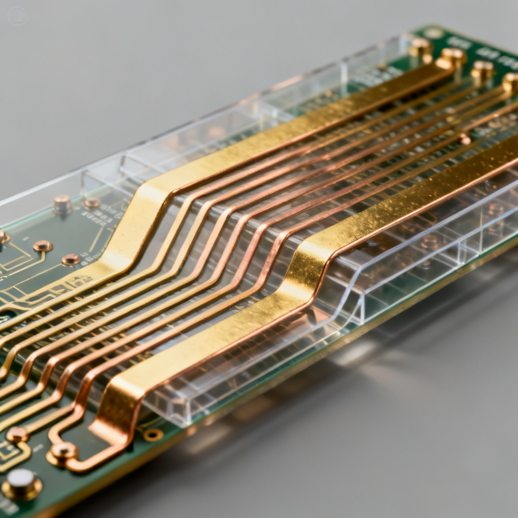
In high-speed digital interfaces like DDR4/DDR5, PCIe Gen4/Gen5, or USB 3.x, maintaining tight impedance tolerance (±10% or better) is critical. When routing these signals through narrow BGA escape areas or under components, tapered traces help maintain the target impedance across the entire path. This is especially important for differential pairs, where both traces must be tapered symmetrically to preserve differential impedance.
How to Design Tapered Traces: Practical Guidelines
Designing an effective taper requires careful calculation and simulation. Here are the step-by-step guidelines from industry experts:
Determine the Required Impedance Transformation
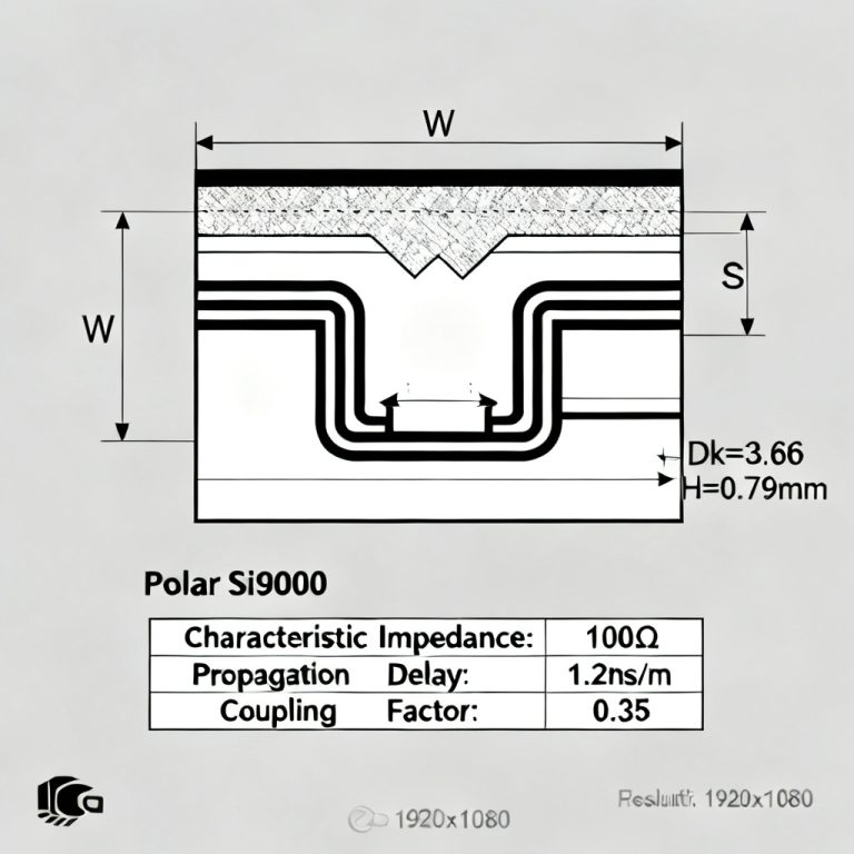
First, calculate the characteristic impedance of both the wider and narrower trace segments using a field solver (e.g., Polar SI9000, HyperLynx, or open-source tools). For example:
- Wide trace (W1): 10 mils → Z₀ = 50Ω
- Narrow trace (W2): 4 mils → Z₀ = 65Ω (assuming same stackup)
Your taper must smoothly transition from 50Ω to 65Ω. Note: The taper itself does not change impedance linearly; the impedance at any point along the taper depends on the local trace width.
Choose the Taper Profile
The most common and recommended profile is the linear taper, where the trace width changes at a constant rate. This is easy to manufacture and provides adequate performance for most high-speed digital applications (up to 10-20 GHz). For RF applications, an exponential taper (Klopfenstein taper) can provide a better impedance match over a wider bandwidth, but it is harder to fabricate and requires precise simulation.
Calculate the Taper Length
This is the most critical parameter. The general rule of thumb is:
- For digital signals: The taper length should be at least 3 to 5 times the maximum trace width (the wider end). For example, if W1 = 10 mils, the taper should be at least 30-50 mils long. Some experts recommend a minimum of 10-20 mils for BGA fan-outs.
- For RF signals: The taper should be a quarter-wavelength (λ/4) at the frequency of interest. For a 2.4 GHz signal (λ ≈ 5 inches in FR4), a λ/4 taper would be about 1.25 inches. Longer tapers (e.g., λ/2) provide even better low-frequency performance.
- Simulation is key: Always use a 2D or 3D electromagnetic simulator to verify the taper’s performance. The goal is to achieve a return loss (S11) better than -20 dB across the operating frequency band.
Avoid Sharp Corners
Ensure that the transition from the taper to the constant-width trace is smooth. Use a small radius (e.g., 2-5 mils) at the start and end of the taper to prevent sharp corners that can act as stress risers and cause manufacturing defects (e.g., under-etching or copper lifting).
Consider the Return Path
For differential pairs, both traces must be tapered identically and symmetrically. Additionally, the ground plane underneath the taper must remain continuous and unbroken. Any split in the reference plane will create a larger impedance discontinuity than the taper itself.
Manufacturing Considerations for Tapered Traces
Tapered traces, while effective, introduce manufacturing challenges that must be addressed to ensure yield and reliability.
Etching Tolerance
Standard PCB etching processes have a tolerance of ±20% for trace width. For a tapered trace, this tolerance can cause the taper to become non-linear or even produce a “neck” where the width changes too rapidly. To mitigate this:
- Use a larger taper length: This reduces the sensitivity to etching variations.
- Specify tighter etching tolerances: Communicate with your PCB manufacturer (like us) to ensure they can achieve ±10% or better for critical high-speed layers.
- Avoid very narrow tapers: If the narrow end is less than 3 mils, consider using a different stackup or a microvia-in-pad solution.
Copper Thickness Variation
Thicker copper (e.g., 2 oz or more) makes etching more difficult because the sidewall etch angle becomes steeper. For tapered traces, use 1 oz (1.4 mil) or 0.5 oz (0.7 mil) copper to ensure a clean, gradual transition. If thicker copper is required (e.g., for high-current power traces), consider using a 45-degree chamfered taper instead of a linear one, which is more forgiving to etching.
Solder Mask and Surface Finish
Solder mask can affect impedance if applied over the taper. To avoid this:
- Use “solder mask defined” (SMD) pads only where necessary. For tapered traces, prefer “non-solder mask defined” (NSMD) pads to keep the copper geometry clean.
- If using ENIG or HASL surface finish, ensure the nickel or tin thickness does not significantly alter the trace profile. ENIG’s nickel layer (typically 150-300 μin) can add a “bump” at the transition point, so account for this in your impedance calculations.
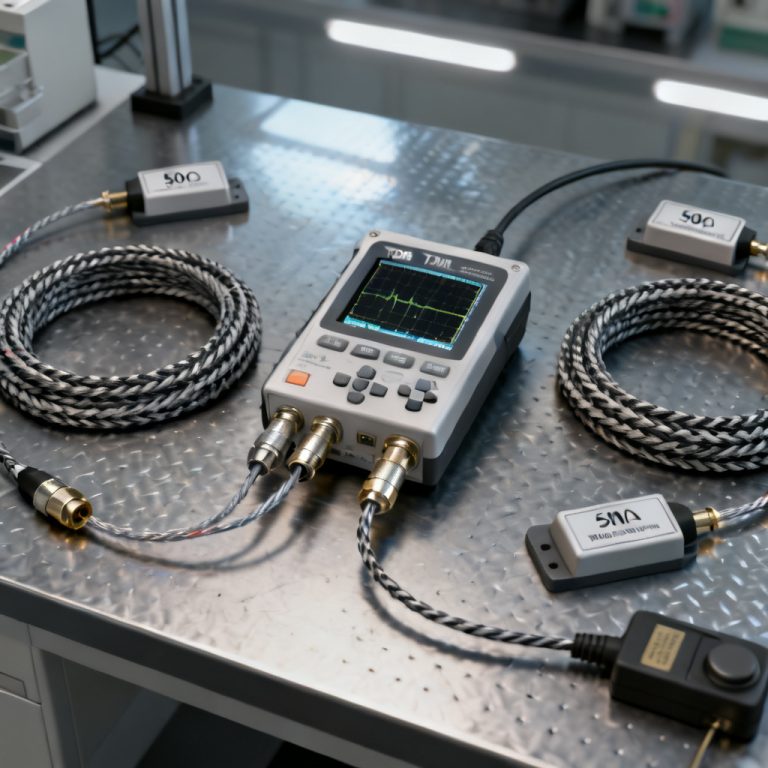
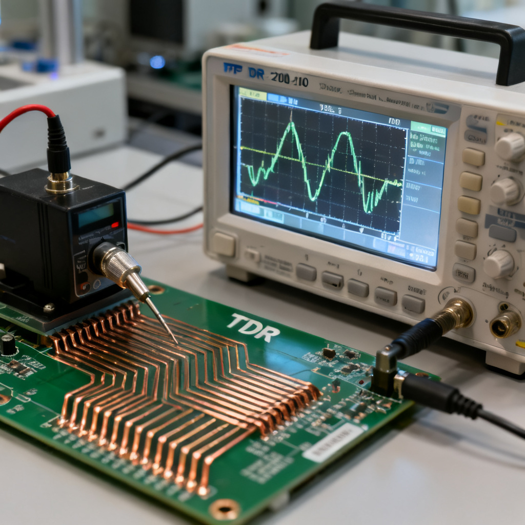
Impedance Testing
After manufacturing, verify the impedance of the tapered trace using TDR (Time Domain Reflectometry). A well-designed taper should show a smooth impedance transition with no sharp spikes. The measured impedance should be within ±10% of the target at both ends. If you see a “dip” or “peak” at the taper location, the length or profile may need adjustment.
Advanced Topics and Best Practices
Tapered Traces vs. Other Impedance Control Methods
- Via stitching: Adding ground vias near a trace can reduce impedance, but it does not provide a smooth transition like a taper.
- Coplanar waveguide (CPW): For very high frequencies (e.g., mmWave), CPW structures with ground planes on the same layer can be tapered more effectively than microstrip.
- Back-drilling: For via stubs, back-drilling removes the unused portion of the via, but it does not address trace width changes.
Simulation-Driven Design
For designs above 5 GHz, always simulate the taper using full-wave 3D EM software (e.g., ANSYS HFSS, CST Microwave Studio). Key parameters to optimize:
- Insertion loss (S21): Should be as close to 0 dB as possible.
- Return loss (S11): Below -20 dB for the entire frequency range.
- Group delay: Should be flat across the band to avoid signal distortion.
Common Mistakes to Avoid
- Making the taper too short: This defeats the purpose and creates a sharp discontinuity.
- Ignoring the ground plane: A gap or slot in the reference plane under the taper will ruin impedance control.
- Using a taper for DC or low-speed signals: Unnecessary and adds cost.
- Not accounting for manufacturing tolerances: Always design with a margin (e.g., +20% length) to ensure success.
Tapered Traces Specifications Table
| Parameter | Tapered Traces Specification | Recommendation |
|---|---|---|
| Trace Width (W1) | Wider end (e.g., 10 mils) | Match target impedance (e.g., 50Ω) |
| Trace Width (W2) | Narrower end (e.g., 4 mils) | Match component pad or routing constraint |
| Taper Length (Digital) | 3-5x W1 | Minimum 30-50 mils |
| Taper Length (RF) | λ/4 | Use quarter-wavelength at operating frequency |
| Etching Tolerance | ±10% or better | Specify to manufacturer |
| Copper Weight | 0.5 oz or 1 oz | For clean etching |
| Impedance Tolerance | ±10% | Verify with TDR |
Tapered Traces vs. Abrupt Width Changes: A Comparison
| Feature | Tapered Traces | Abrupt Width Changes |
|---|---|---|
| Impedance Continuity | Gradual transition, minimal reflection | Sharp discontinuity, high reflection |
| Signal Integrity | Preserved at high frequencies | Degraded with ringing and crosstalk |
| Manufacturing Complexity | Moderate (requires precise etching) | Low (simple geometry) |
| Application | High-speed digital, RF, BGA fan-outs | Low-speed, DC, non-critical paths |
Glossary of Key Terms
- Characteristic Impedance (Z₀): The constant impedance of a transmission line, determined by geometry and dielectric properties.
- Impedance Mismatch: A difference between the impedance of a transmission line and its load or source, causing reflections.
- Return Loss (S11): A measure of how much signal power is reflected back due to impedance discontinuities.
- VSWR (Voltage Standing Wave Ratio): The ratio of maximum to minimum voltage on a transmission line, indicating mismatch.
- Quarter-Wave Transformer: A transmission line segment of length λ/4 used to match two different impedances.
Frequently Asked Questions (FAQ)
What are tapered traces in impedance control PCB design?
Tapered traces are gradual width transitions used in impedance control PCB design to smoothly change trace width while minimizing impedance mismatch, crucial for high-speed signal integrity.
When should I use tapered traces?
Use tapered traces when connecting to BGA pads, routing between different impedance zones, in RF circuits, or for high-speed digital buses like DDR and PCIe to maintain consistent impedance.
How do I calculate the length of a tapered trace?
For digital signals, use 3-5 times the maximum trace width; for RF signals, use a quarter-wavelength (λ/4) at the operating frequency. Always simulate for best results.
Can tapered traces be manufactured easily?
Yes, but they require tighter etching tolerances (e.g., ±10%) and careful selection of copper weight (0.5 oz or 1 oz) to avoid defects. Work closely with your PCB manufacturer.
What is the difference between linear and exponential tapers?
Linear tapers change width at a constant rate and are easier to manufacture; exponential tapers (Klopfenstein) provide wider bandwidth impedance matching but are harder to fabricate.
“`