The demand for higher data rates in data centers and high-performance computing has driven the adoption of PAM4 signaling at 112 Gbps. To design an impedance control PCB for PAM4 signaling, engineers must address tighter noise margins, extreme loss management, and precise manufacturing tolerances. This guide provides a complete framework for achieving reliable 112G performance.

Material Selection for Impedance Control PCB for PAM4 Signaling
Standard FR-4 is unsuitable for an impedance control PCB for PAM4 signaling at 112G. The substrate must exhibit an ultra-low dissipation factor (Df) between 0.002 and 0.005 at 10 GHz. A stable dielectric constant (Dk) with a tolerance of ±0.05 is critical for consistent impedance. The glass weave effect introduces Dk variations; using spread glass or very low profile (VLP) glass minimizes this. Recommended material families include MEGTRON 6/7, ROGERS 3000 series, ISOLA Tachyon 100G, and NELCO N4000-13 SI EP. The copper foil must be VLP or hyper VLP (HVLP) to reduce conductor loss from surface roughness. These choices directly impact the impedance control PCB for PAM4 signaling performance.
Key Material Parameters
The dissipation factor (Df) measures signal energy lost as heat. For 112G PAM4, a Df below 0.005 is mandatory. The dielectric constant (Dk) must remain stable across frequency and temperature. The glass weave effect creates localized Dk variations; spread glass reduces this. Copper foil roughness contributes to conductor loss, so VLP or HVLP foil is essential.
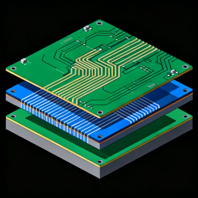
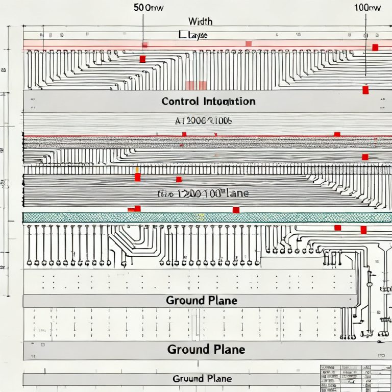
Stack-Up Design for Impedance Control PCB for PAM4 Signaling
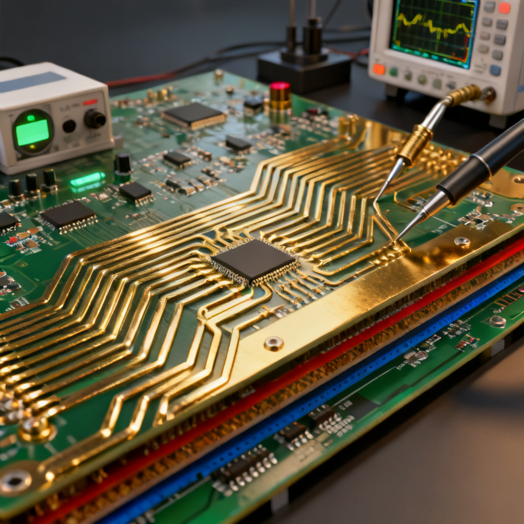
A symmetrical stack-up is mandatory for an impedance control PCB for PAM4 signaling. Asymmetry causes warping during lamination, leading to unpredictable impedance variations. Stripline topology is preferred for inner layers because it provides a shielded environment with lower crosstalk. Reference plane integrity must be maintained with no gaps under high-speed traces. Stitching vias ensure a continuous return path when changing layers. The following rules guide the stack-up design for an impedance control PCB for PAM4 signaling.
Critical Stack-Up Rules
Symmetry requires identical copper weight, core thickness, and prepreg type on mirrored layers. Stripline offers superior control compared to microstrip, which is more susceptible to surface roughness and soldermask effects. Reference planes must be continuous; any split creates impedance discontinuity. Minimum plane clearance should be three times the dielectric height from the trace.
Example 16-Layer Stack-Up for 112G
| Layer | Material | Purpose |
|---|---|---|
| 1 | Copper + Soldermask | Top Signals (Microstrip) |
| 2 | Ground Plane | Return Path |
| 3 | Signal | 112G Stripline |
| 4 | Ground Plane | Return Path |
| 5 | Power | Power Plane |
| 6 | Ground Plane | Return Path |
| 7 | Signal | 112G Stripline |
| 8 | Ground Plane | Return Path |
| 9 | Ground Plane | Return Path |
| 10 | Signal | 112G Stripline |
| 11 | Power | Power Plane |
| 12 | Ground Plane | Return Path |
| 13 | Signal | 112G Stripline |
| 14 | Ground Plane | Return Path |
| 15 | Ground Plane | Return Path |
| 16 | Copper + Soldermask | Bottom Signals |
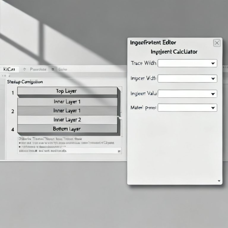
Trace Geometry and Impedance Calculation for Impedance Control PCB for PAM4 Signaling
For an impedance control PCB for PAM4 signaling, generic calculators are insufficient. Use 2D field solvers like Polar Si9000 or Ansys Q3D that account for exact stack-up materials. Key parameters for 100Ω differential impedance include trace width (typically 4-6 mils), trace spacing greater than width, dielectric height as the primary control variable, and copper thickness of 0.5 oz or 1 oz. Maintaining constant separation along the entire differential pair is critical. Avoid necking down trace width at connector pads; use tapered pads instead. This ensures consistent impedance control PCB for PAM4 signaling performance.
Differential Pair Design Rules
The spacing between traces in a differential pair must remain constant. Any variation introduces impedance mismatch. Necking down at pads creates a local discontinuity. Tapered or dog-bone pads mitigate this effect. These rules are essential for maintaining signal integrity in an impedance control PCB for PAM4 signaling.
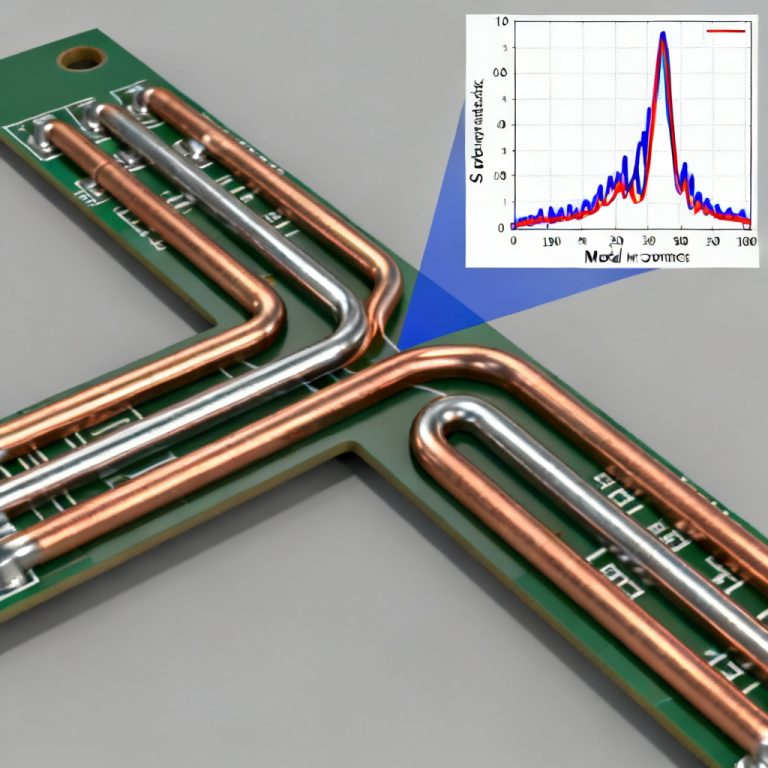
Via Design and Backdrilling for Impedance Control PCB for PAM4 Signaling
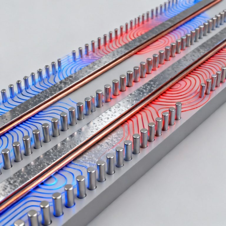
Vias are a major source of impedance discontinuity in an impedance control PCB for PAM4 signaling. The unused portion of a via barrel, called the stub, acts as a transmission line stub and creates a resonant null in insertion loss. Backdrilling removes this stub. The residual stub must be less than 10 mils (0.25 mm) to push the resonant frequency above 28 GHz. Use the smallest possible via diameter, typically 8-10 mil finished hole size. Place ground vias around signal vias to create a coaxial-like structure. Microvias and HDI technology can eliminate via stubs entirely. These techniques are critical for an impedance control PCB for PAM4 signaling.
Backdrilling Design Rules
The residual stub after backdrilling must be below 10 mils. Use microvias for layer transitions when possible. For through-hole vias, specify the smallest drill size that can be reliably backdrilled. Via fences with ground vias reduce impedance mismatch. These rules ensure that vias do not degrade the impedance control PCB for PAM4 signaling performance.
Surface Finish and Soldermask for Impedance Control PCB for PAM4 Signaling
The surface finish affects high-frequency performance, especially for microstrip lines. ENIG is not recommended for 112G microstrip because the nickel layer introduces magnetic loss. Immersion silver and OSP are preferred for their low loss. Hard gold is suitable only for edge connectors. Soldermask has a high Dk and Df, which shifts impedance. Removing soldermask from critical microstrip traces (windowed) restores the calculated impedance. Low-loss soldermask is an alternative. These choices are vital for an impedance control PCB for PAM4 signaling.
Surface Finish Comparison
| Surface Finish | High-Frequency Performance | Recommendation for 112G |
|---|---|---|
| ENIG | Poor due to nickel layer | Avoid |
| Immersion Silver | Excellent | Recommended |
| Immersion Tin | Good | Acceptable with caution |
| OSP | Very low loss | Recommended |
| Hard Gold | Good for contacts | Edge connectors only |
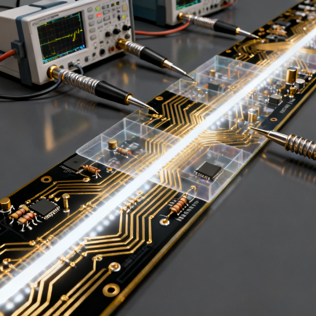
Simulation and Verification for Impedance Control PCB for PAM4 Signaling
Simulation is essential before fabrication of an impedance control PCB for PAM4 signaling. Use 2D field solvers for each unique trace geometry to calculate exact impedance. 3D EM simulation (HFSS, CST) models the entire channel, including connector footprints, traces, and vias. Key metrics include insertion loss (less than -10 dB at 28 GHz), return loss (better than -10 dB), and crosstalk (less than -30 dB). Time domain reflectometry (TDR) provides a physical impedance profile. These verification steps ensure the impedance control PCB for PAM4 signaling meets performance targets.
Required Simulations
2D field solvers calculate impedance for each trace geometry. 3D EM simulation evaluates the complete channel. TDR measurement identifies impedance discontinuities. These tools are indispensable for an impedance control PCB for PAM4 signaling.
Comparison: Our Capabilities for Impedance Control PCB for PAM4 Signaling
We specialize in manufacturing impedance control PCB for PAM4 signaling with advanced capabilities. Our ultra-low loss material lamination supports MEGTRON, Rogers, and Isola. Precision backdrilling achieves residual stubs below 5 mils. Impedance control is maintained to ±3%. VLP and HVLP copper foil are standard. Immersion silver and OSP surface finishes are available. Full TDR and insertion loss testing verify performance. This expertise ensures your impedance control PCB for PAM4 signaling meets 112G requirements.
Industry Terminology
PAM4 (Pulse Amplitude Modulation with 4 levels) transmits 2 bits per symbol using four voltage levels. Insertion loss is the signal power lost as it travels through the PCB. Return loss measures reflections caused by impedance mismatches. Backdrilling removes the unused portion of a via barrel to eliminate stub resonance. Stripline is a transmission line embedded between two reference planes. Understanding these terms is fundamental to designing an impedance control PCB for PAM4 signaling.
Frequently Asked Questions About Impedance Control PCB for PAM4 Signaling
What is an impedance control PCB for PAM4 signaling?
An impedance control PCB for PAM4 signaling is a printed circuit board designed with precise trace geometries and materials to maintain a consistent characteristic impedance, typically 100Ω differential, for 112G PAM4 signals. This ensures minimal reflections and signal degradation.
Why is material selection critical for impedance control PCB for PAM4 signaling?
Material selection is critical because the dielectric constant and dissipation factor directly affect impedance and signal loss. Ultra-low loss materials with stable Dk are required to maintain impedance tolerance and minimize insertion loss at 28 GHz.
How does backdrilling improve impedance control PCB for PAM4 signaling?
Backdrilling removes the via stub, which otherwise creates a resonant null in insertion loss. This improves impedance matching and reduces reflections, which is essential for maintaining signal integrity in an impedance control PCB for PAM4 signaling.
What surface finish is best for impedance control PCB for PAM4 signaling?
Immersion silver and OSP are the best surface finishes for impedance control PCB for PAM4 signaling due to their low loss at high frequencies. ENIG should be avoided because the nickel layer increases loss.