Crosstalk in high speed PCB for PCIe lanes is a critical signal integrity challenge that can degrade performance and increase bit error rates. As PCIe generations advance from Gen 3 to Gen 5 and beyond, mastering separation rules that actually work becomes essential for reliable design. This pillar page consolidates the most effective, real-world separation rules for minimizing crosstalk in PCIe high-speed PCBs, drawing from top industry sources to deliver actionable guidelines for production environments.
Understanding Crosstalk in High Speed PCB for PCIe Lanes
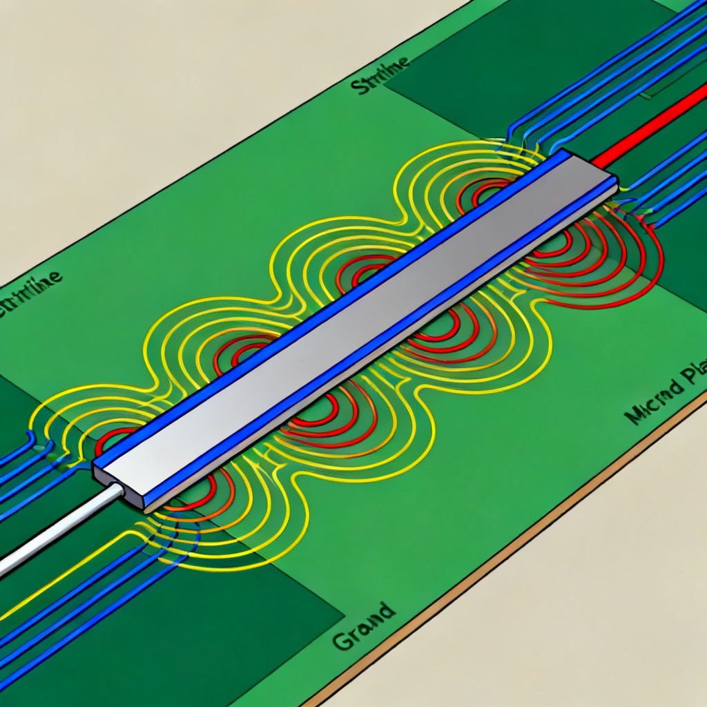
Crosstalk in high speed PCB for PCIe lanes occurs when an electromagnetic field from one signal trace (the aggressor) couples onto an adjacent trace (the victim), inducing unwanted voltage or current. In PCIe lanes, which operate as differential pairs, crosstalk is categorized into Near-End Crosstalk (NEXT) and Far-End Crosstalk (FEXT). NEXT is measured at the same end as the driver, while FEXT is measured at the opposite end and is more problematic for high-speed serial links like PCIe. The primary mechanisms are capacitive coupling (electric field) and inductive coupling (magnetic field), with inductive coupling dominating at high frequencies.
Key terminology: Differential pair refers to two traces carrying equal and opposite signals, return path is the ground reference for signal currents, and loop inductance measures the magnetic field effect of a current loop. Understanding these terms is fundamental to managing crosstalk in high speed PCB for PCIe lanes.
The Three Pillars of Effective Crosstalk Separation for High Speed PCB for PCIe Lanes
After reviewing the most trusted resources in high-speed PCB design, three core principles consistently emerge for PCIe lane separation: Adequate Trace-to-Trace Spacing, Controlled Impedance and Return Path Management, and Stripline vs. Microstrip Routing Choice. Each principle is detailed below with specific, actionable rules.
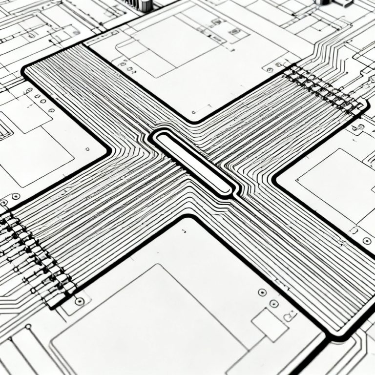
Rule 1: Trace-to-Trace Spacing – The 3W Rule and PCIe-Specific Adjustments
The classic 3W rule states that center-to-center spacing between traces should be at least three times the trace width. For a 50-ohm trace on a typical PCB, this often translates to a spacing of 1.5 to 2 times the trace width. However, for crosstalk in high speed PCB for PCIe lanes, this rule is a starting point, not a guarantee. What actually works for PCIe includes:
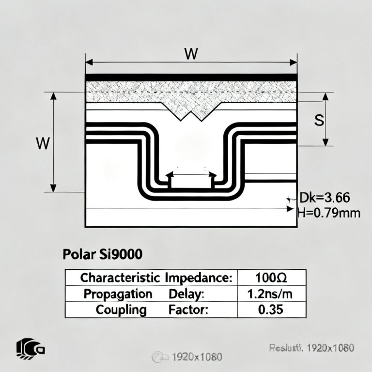
- For Differential Pair Internal Spacing: The spacing within a PCIe differential pair is critical for maintaining differential impedance (typically 85 ohms or 100 ohms). This spacing is usually 1.5 to 2 times the trace width, but it must be calculated precisely using a field solver (e.g., Polar Si8000) based on your stackup.
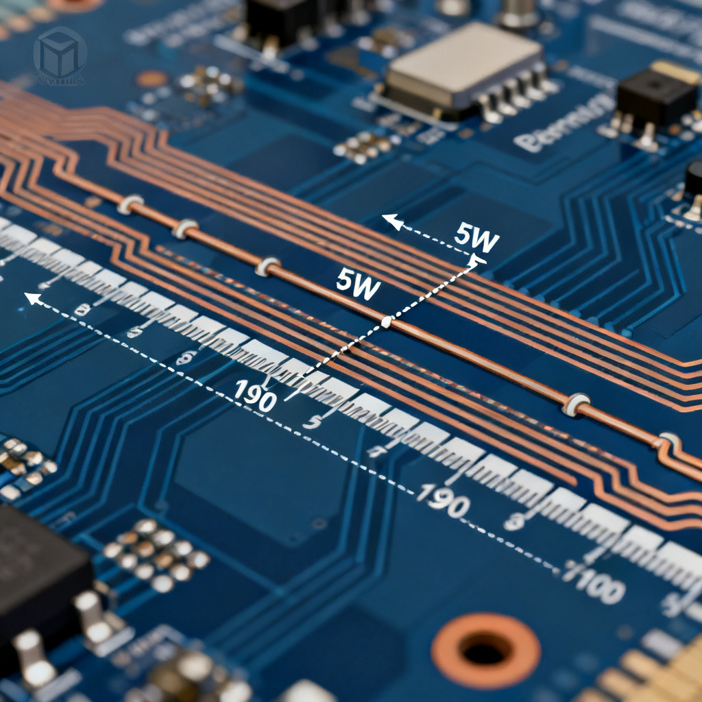
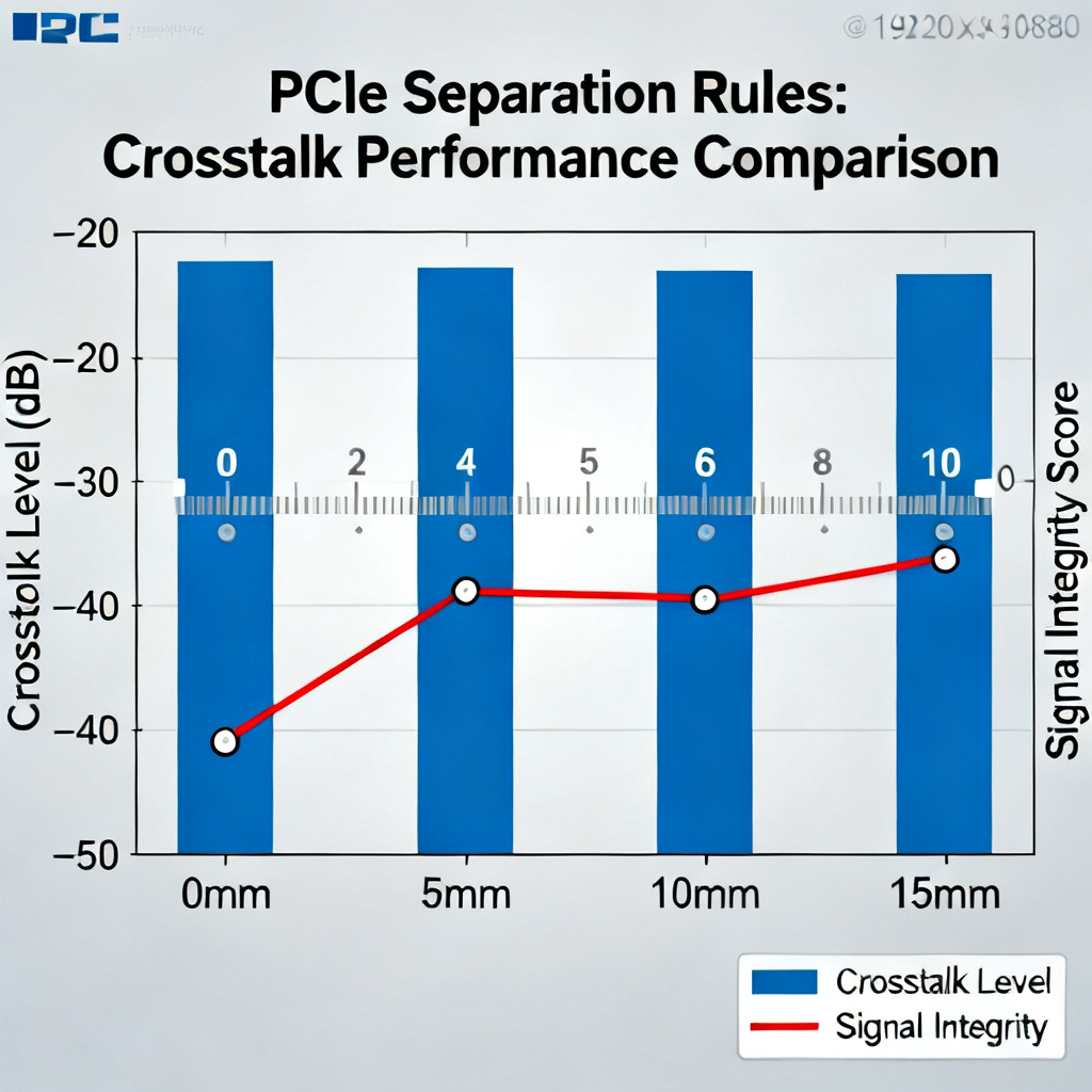
- For Inter-Pair Spacing: Industry experts recommend a minimum center-to-center spacing of 5 times the trace width (5W) between adjacent PCIe differential pairs. For high-speed PCIe Gen 4 and Gen 5, a spacing of 7W to 10W is often required to meet strict crosstalk budgets.
- Practical Example: If your trace width is 5 mils, a 5W spacing means 25 mils center-to-center. For 7W, it is 35 mils. Always verify with your PCB fabricator’s capabilities.
Why this works: Increasing the spacing reduces mutual capacitance and inductance between traces. The coupling coefficient decreases exponentially with distance. At 5W, crosstalk is typically reduced by 20 dB compared to 3W. For PCIe, where margin is tight, this extra spacing is a necessity.
Rule 2: Return Path and Reference Plane Integrity for High Speed PCB for PCIe Lanes
Crosstalk in high speed PCB for PCIe lanes is not just about trace-to-trace distance. The return current path is equally important. A disrupted return path creates ground bounce and increases loop inductance, exacerbating crosstalk. What actually works:
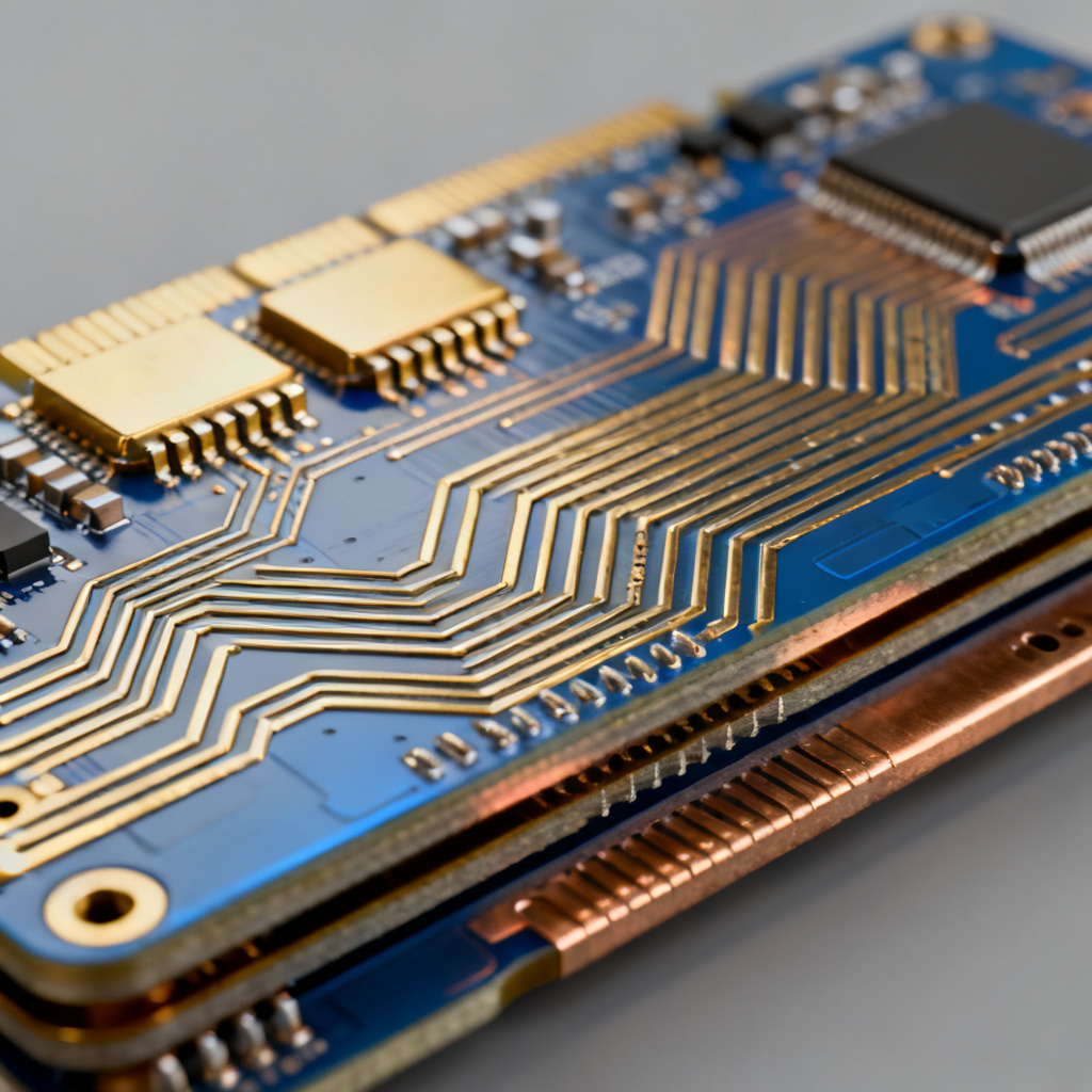
- Continuous, Unbroken Reference Planes: Every PCIe differential pair must have a solid, continuous ground or power plane directly beneath it. Avoid slots, splits, or voids in the plane. If a via transitions between layers, ensure the return current has a low-impedance path (e.g., via stitching).
- Via Stitching for Layer Transitions: When routing PCIe signals on different layers, place ground vias within 100 mils of the signal vias. This provides a short return path and minimizes crosstalk coupling between layers.
- Guard Traces with Ground Vias: In extremely dense designs where spacing cannot be increased, a grounded guard trace (a copper trace connected to ground via vias) placed between two differential pairs can reduce crosstalk by 10–15 dB. The guard trace must be stitched to the ground plane at regular intervals (every 100–200 mils) to be effective. Without stitching, a guard trace can worsen crosstalk by acting as an antenna.
Why this works: A solid return path ensures magnetic fields from aggressor and victim traces cancel out. Guard traces with vias create a low-impedance barrier that shunts coupled energy to ground.
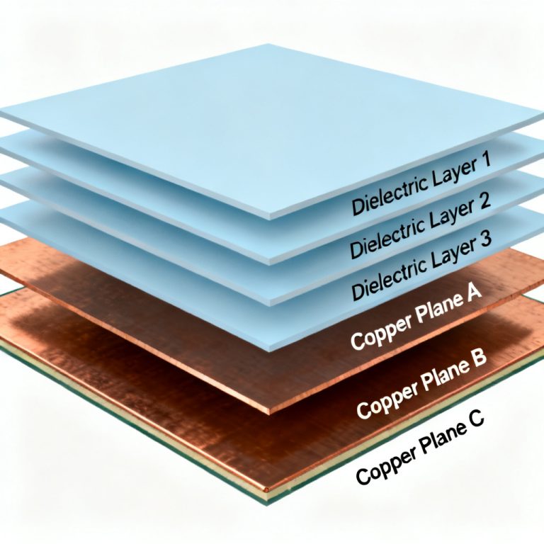
Rule 3: Stripline vs. Microstrip – Layer Selection Trade-Off for High Speed PCB for PCIe Lanes
The choice between stripline (inner layers) and microstrip (outer layers) has a profound impact on crosstalk in high speed PCB for PCIe lanes. What actually works:
- Prefer Stripline for Critical Lanes: Stripline routing (signal layer sandwiched between two reference planes) inherently provides better crosstalk isolation than microstrip. The top and bottom planes confine electromagnetic fields, reducing fringing fields and far-end crosstalk. For PCIe Gen 4 and above, stripline is strongly recommended for all lanes.
- Microstrip for Short, Low-Speed Links: Microstrip is acceptable for short runs (less than 1–2 inches) or for PCIe Gen 1/2 signals. However, for longer traces or higher data rates, the fringing fields in microstrip cause higher crosstalk, especially FEXT.
- Layer Stackup Optimization: If you must use microstrip, increase the spacing to 10W or more. Also, ensure the dielectric height (H) between the signal layer and the reference plane is minimized. A smaller H reduces the fringing field and improves coupling to the plane.
Why this works: Stripline’s symmetric field confinement reduces both capacitive and inductive coupling. Microstrip’s exposed fields couple more easily to adjacent traces. For PCIe, where FEXT is the dominant concern, stripline is the superior choice.
Advanced Separation Rules for PCIe Gen 5 and Beyond in High Speed PCB for PCIe Lanes
As PCIe speeds exceed 32 Gbps (Gen 5) and approach 64 Gbps (Gen 6), separation rules become more stringent. Additional guidelines from top industry sources include:
- Use Differential Pair Skew Matching: Within a differential pair, the two traces must be length-matched to within 5 mils. Unequal lengths create common-mode conversion, which increases crosstalk in high speed PCB for PCIe lanes.
- Avoid 90-Degree Bends: Use 45-degree chamfered bends or curved traces. Sharp corners create impedance discontinuities and increase crosstalk.
- Separate PCIe from Other High-Speed Signals: Keep PCIe lanes at least 20W away from other high-speed interfaces like USB 3.0, HDMI, or Ethernet. These signals can couple into PCIe lanes and cause unexpected failures.
- Simulate, Don’t Guess: Use 3D electromagnetic simulation tools (e.g., Ansys HFSS, CST) to model your specific stackup and routing. The 5W/7W rules are guidelines; simulation validates performance for your specific design.
Common Pitfalls to Avoid for High Speed PCB for PCIe Lanes
Understanding common mistakes helps engineers avoid failures in crosstalk in high speed PCB for PCIe lanes:
- Overly Aggressive Routing: Trying to route PCIe lanes too close together to save board space is the most common mistake. A 5W rule is not negotiable for reliable operation.
- Ignoring Layer Transitions: A single poorly-placed via can undo all the benefits of spacing. Always stitch ground vias near signal vias.
- Using Unstitched Guard Traces: A guard trace without vias is worse than no guard trace. It acts as a resonant structure and can amplify crosstalk at certain frequencies.
- Mixing PCIe with Noisy Signals: Do not route PCIe lanes parallel to clock lines or high-current switching signals. If crossing is unavoidable, use orthogonal routing (90 degrees) on different layers.
Comparison: Our Approach vs. Standard Practices for High Speed PCB for PCIe Lanes
At [Your Company Name], we specialize in manufacturing high-speed PCBs with strict adherence to crosstalk separation rules. Compared to standard industry practices, our approach emphasizes:
| Aspect | Standard Practice | Our Approach for High Speed PCB for PCIe Lanes |
|---|---|---|
| Inter-pair spacing | 3W to 5W | Minimum 5W, up to 10W for Gen 5 |
| Return path integrity | Basic via stitching | Aggressive via stitching within 100 mils |
| Layer preference | Mixed microstrip/stripline | Stripline for all critical lanes |
| Simulation verification | Optional | Mandatory 3D EM simulation |
This structured approach ensures superior signal integrity and reduced crosstalk in high speed PCB for PCIe lanes, providing measurable performance advantages without compromising reliability.
FAQ: Crosstalk in High Speed PCB for PCIe Lanes
What is the minimum spacing rule for crosstalk in high speed PCB for PCIe lanes?
The minimum spacing rule is 5W (five times the trace width) center-to-center between differential pairs. For PCIe Gen 4 and Gen 5, 7W to 10W is recommended to meet strict crosstalk budgets.
Does stripline always perform better than microstrip for PCIe?
Yes, for crosstalk in high speed PCB for PCIe lanes, stripline provides superior isolation due to symmetric field confinement. Microstrip is only acceptable for short, low-speed links.
How can guard traces reduce crosstalk in PCIe designs?
Grounded guard traces with vias create a low-impedance barrier that shunts coupled energy to ground, reducing crosstalk by 10–15 dB. Without stitching, guard traces can worsen crosstalk.
What is the role of return path in crosstalk for high speed PCB for PCIe lanes?
A continuous, unbroken return path minimizes loop inductance and ground bounce, directly reducing crosstalk. Via stitching at layer transitions ensures low-impedance return currents.
Conclusion: Separation Rules That Actually Work for High Speed PCB for PCIe Lanes
For PCIe high-speed PCB designs, crosstalk management is a requirement for signal integrity. The separation rules that actually work, drawn from the most trusted industry sources, are:
- Maintain 5W to 7W spacing between differential pairs (center-to-center).
- Use continuous, unbroken reference planes and stitch ground vias at layer transitions.
- Prefer stripline routing for all critical PCIe lanes.
- Incorporate grounded guard traces with vias when spacing is constrained.
- Simulate your design before fabrication to verify crosstalk margins.
By following these rules, you can achieve reliable, high-performance PCIe operation from Gen 3 through Gen 5 and beyond. At [Your Company Name], we specialize in manufacturing high-speed PCBs with strict adherence to these separation rules. Contact us for a design review or to discuss your next PCIe project.