In high-speed PCB design, Impedance Control PCB Design Rule Checking is critical for signal integrity. Automating this in EDA tools ensures first-pass success for your Impedance Control PCB Design Rule Checking workflow. This guide covers everything from stackup to manufacturing handoff.

Understanding Impedance Control Parameters for Impedance Control PCB Design Rule Checking
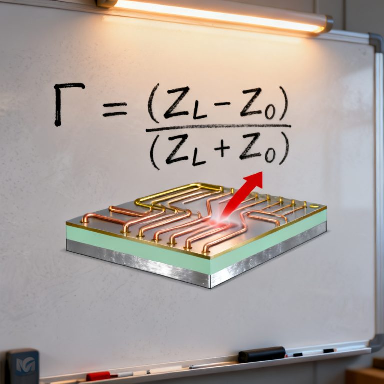
Before automating Impedance Control PCB Design Rule Checking, you must understand the variables that determine characteristic impedance (Z0). These parameters directly affect your Impedance Control PCB Design Rule Checking results.
Key Variables Influencing Impedance
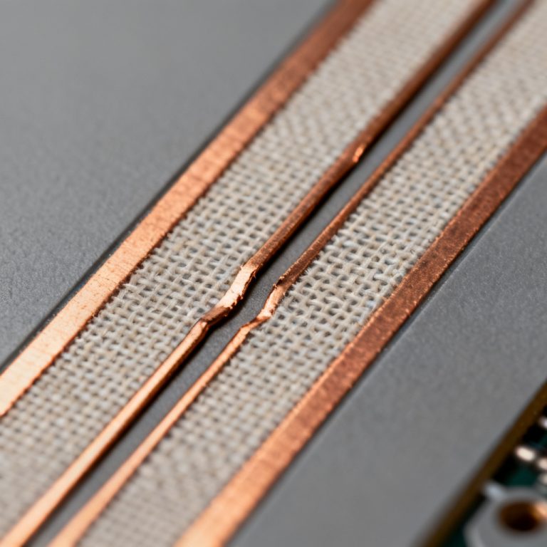
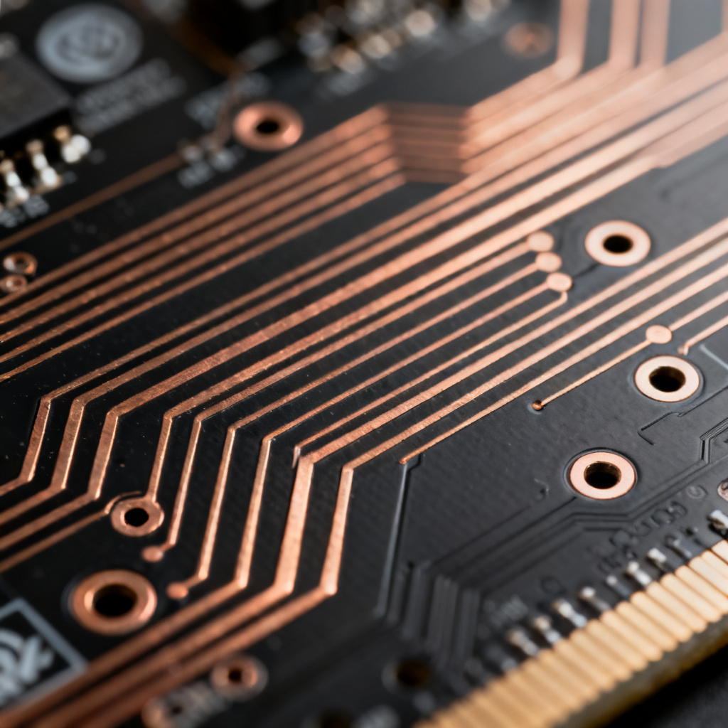
Impedance Control PCB Design Rule Checking relies on trace width (W), dielectric height (H), dielectric constant (Er), copper thickness (T), and solder mask thickness. Each variable must be accurately modeled in your EDA tool for effective Impedance Control PCB Design Rule Checking.
Microstrip vs. Stripline Topologies
Microstrip offers easier manufacturing but less controlled impedance. Stripline provides better isolation. Both require precise Impedance Control PCB Design Rule Checking to meet target values.
Differential Impedance
For differential pairs, Impedance Control PCB Design Rule Checking must enforce both trace width (W) and spacing (S) to achieve target Zdiff (e.g., 100Ω).
Automating Impedance Control DRC Rules: Core Parameters
Automated Impedance Control PCB Design Rule Checking includes several rule types that ensure design compliance.
Impedance Target Rules
Define net classes with target impedance (e.g., 50Ω single-ended). Impedance Control PCB Design Rule Checking flags any deviation beyond tolerance.
Trace Width and Spacing Constraints
Impedance Control PCB Design Rule Checking enforces calculated trace width and spacing for both single-ended and differential pairs.
Reference Plane Continuity
Impedance Control PCB Design Rule Checking must verify continuous reference planes under all high-speed traces. Plane voids cause impedance spikes.
Via Impedance and Stub Control
Automated Impedance Control PCB Design Rule Checking includes via stub length checks and backdrill rules for frequencies above 5 Gbps.
Stackup Validation
Impedance Control PCB Design Rule Checking validates the entire stackup against target impedance, including dielectric thickness and copper weight.
EDA Tool Workflows for Impedance Control PCB Design Rule Checking
Each EDA tool offers unique features for Impedance Control PCB Design Rule Checking. Below are step-by-step workflows.
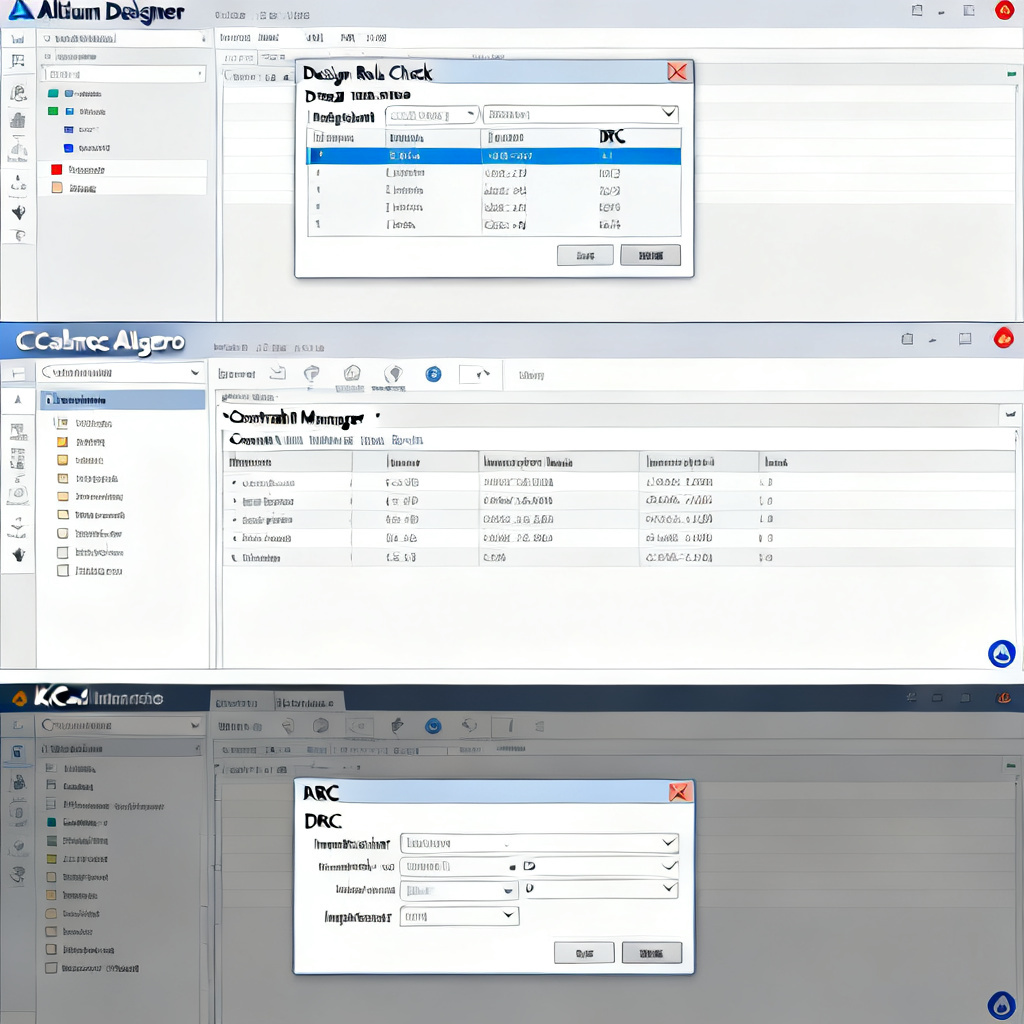
Altium Designer Workflow
Set up stackup with impedance calculation, create net classes, and run DRC. Impedance Control PCB Design Rule Checking in Altium automatically updates width rules when stackup changes.
Cadence Allegro Workflow
Use Constraint Manager for physical rules, enable Impedance Profile, and run Return Path Check. Impedance Control PCB Design Rule Checking in Allegro includes backdrill automation.
KiCad Workflow
Define stackup with impedance control, create net classes, and run DRC. Impedance Control PCB Design Rule Checking in KiCad flags width and clearance violations.
Mentor PADS Workflow
Use Impedance Calculator in Layer Stackup Editor, set net class rules, and run Verify Design for Impedance Control PCB Design Rule Checking.
Advanced Techniques for Impedance Control PCB Design Rule Checking
Expert insights enhance your Impedance Control PCB Design Rule Checking approach.
Solder Mask Modeling
Enable solder mask in impedance calculation. Impedance Control PCB Design Rule Checking must account for 2–5 ohm reduction on outer layers.
Glass Weave Effect
At frequencies above 10 GHz, use spread glass materials. Impedance Control PCB Design Rule Checking flags long traces on single glass weave orientation.
Impedance Coupon Design
Auto-generate impedance coupons matching board stackup. Impedance Control PCB Design Rule Checking ensures coupon geometry matches production traces.
Temperature and Frequency Effects
Set DRC tolerance to ±5% for high-reliability designs. Impedance Control PCB Design Rule Checking uses frequency-dependent material models.
Manufacturing Handoff Report
Include target impedance, calculated trace geometry, stackup details, and DRC results. Impedance Control PCB Design Rule Checking automates report generation.
Common Pitfalls in Impedance Control PCB Design Rule Checking
| Pitfall | Consequence | Solution via Automated Impedance Control PCB Design Rule Checking |
|---|---|---|
| Ignoring via stubs | Signal reflection at 10+ Gbps | Set backdrill rule with max stub length (e.g., 10 mils) |
| Wrong Er value | Impedance off by 10–20% | Use manufacturer-supplied Er for specific material |
| Solder mask not modeled | Impedance reduced by 2–5 ohms | Enable solder mask in stackup impedance calculation |
| Reference plane voids | Impedance spike, EMI | Run return path check for all high-speed nets |
| Asymmetrical stackup | Board warpage, impedance variation | DRC check layer thickness symmetry |
| Mixing material types | Impedance mismatch between layers | Assign unique net classes per material type |
FAQ: Impedance Control PCB Design Rule Checking
What is Impedance Control PCB Design Rule Checking?
Impedance Control PCB Design Rule Checking is an automated process in EDA tools that verifies trace geometry, stackup, and reference plane continuity against target impedance values.
Why automate Impedance Control PCB Design Rule Checking?
Automation reduces design cycles, improves first-pass success, and enhances signal integrity by catching impedance errors early.
Which EDA tools support Impedance Control PCB Design Rule Checking?
Altium Designer, Cadence Allegro, KiCad (v8+), and Mentor PADS all offer features for Impedance Control PCB Design Rule Checking.
How do I set tolerance in Impedance Control PCB Design Rule Checking?
Typical tolerance is ±10% for single-ended and ±15% for differential. For RF designs, ±5% is recommended.
Can Impedance Control PCB Design Rule Checking handle differential pairs?
Yes, most EDA tools include differential pair rules that enforce both trace width and spacing for target Zdiff.