When designing a high-speed digital system, mastering Impedance Control PCB for PCIe 5.0 is the foundation of signal integrity. At 32 GT/s, even a few ohms of mismatch can cause data errors. This guide covers the exact specifications, verification methods, and best practices you need to ensure your PCB performs reliably.
Core Impedance Specifications for PCIe 5.0
Single-Ended Impedance: The 50 Ω Standard
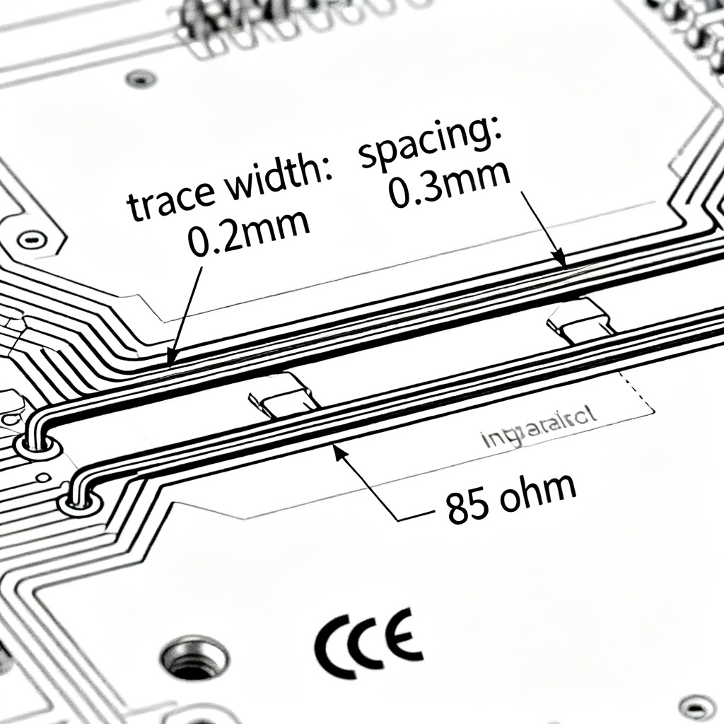
For any Impedance Control PCB for PCIe 5.0, the single-ended impedance target is 50 Ω ± 10% for each individual trace. This value is the industry standard for high-frequency transmission lines, balancing minimal signal loss with practical manufacturing tolerances. Key points include: tolerance of ±10% is standard, and the impedance is defined relative to a continuous reference plane (typically ground).
Differential Impedance: The 85 Ω Requirement
PCIe 5.0 uses differential signaling with a target of 85 Ω ± 10% for the pair. This is a critical shift from PCIe 4.0’s 100 Ω standard, chosen to reduce power consumption and improve signal integrity at 32 GT/s. The lower impedance reduces voltage swing and helps maintain tight jitter control. Always confirm with your specific controller datasheet, but 85 Ω is the default for standard board-to-board designs.
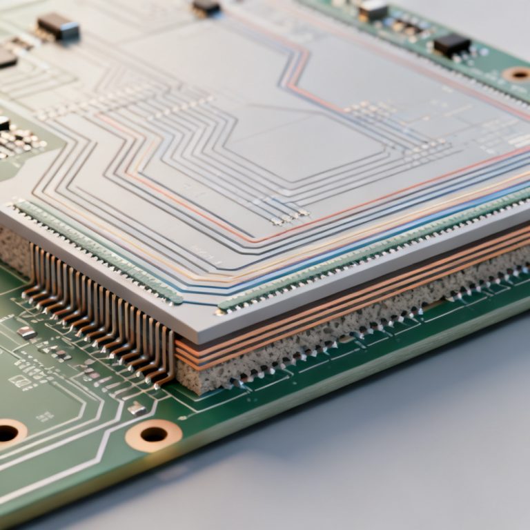
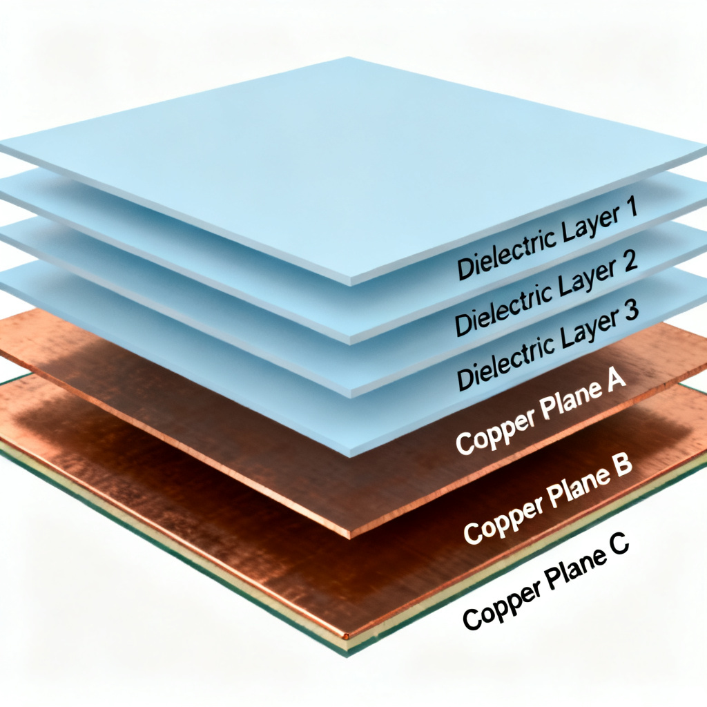
Trace Geometry and Stackup Requirements
To achieve these targets, your stackup must be carefully engineered. Key parameters include trace width (typically 4–8 mils for 50 Ω), trace spacing (5–10 mils for differential pairs), dielectric height (4–6 mils), and copper weight (standard 1 oz). Use a field solver like Polar Si9000 to model your stackup before manufacturing.
How to Verify Impedance Control
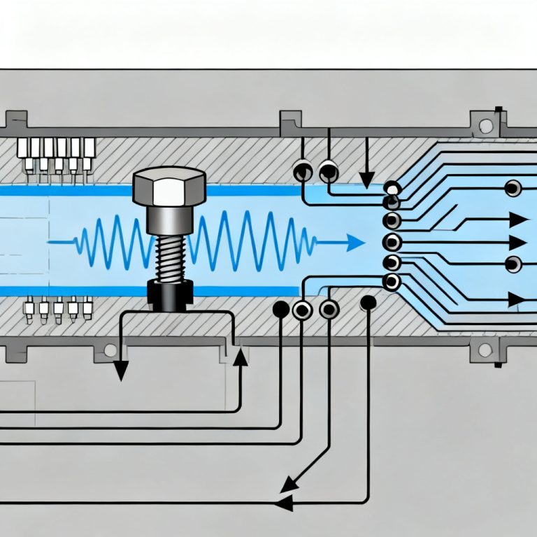
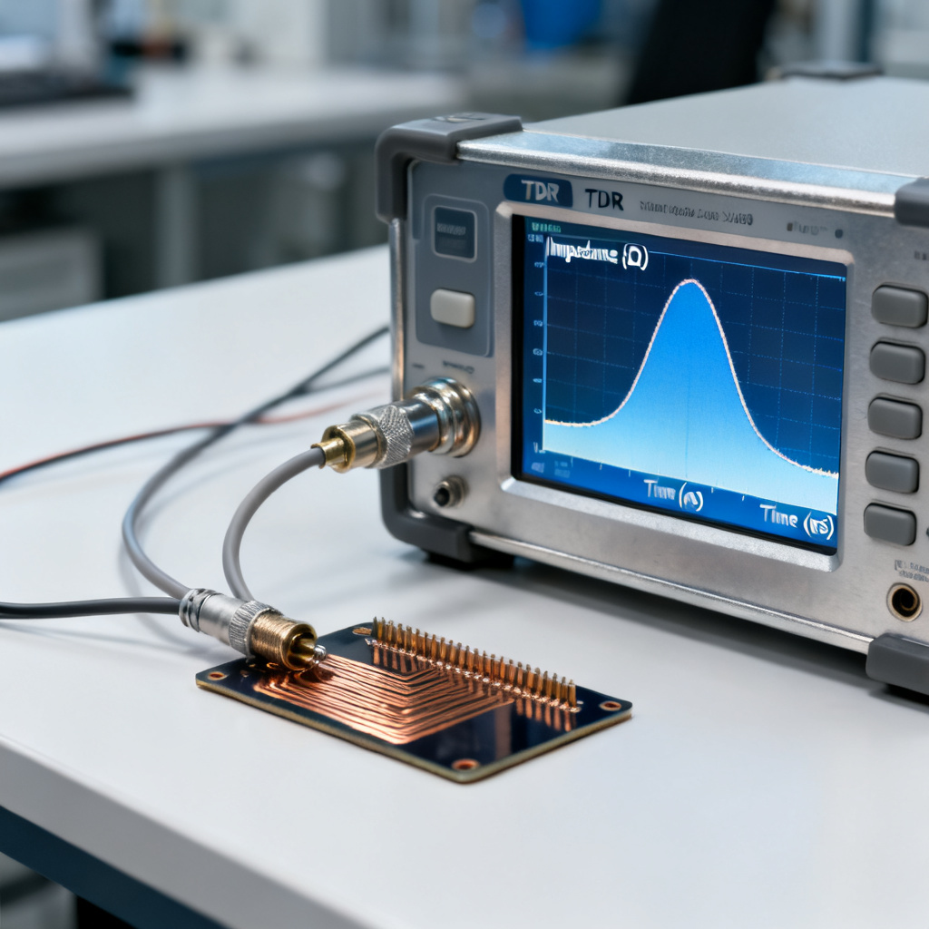
TDR (Time Domain Reflectometry) – The Gold Standard
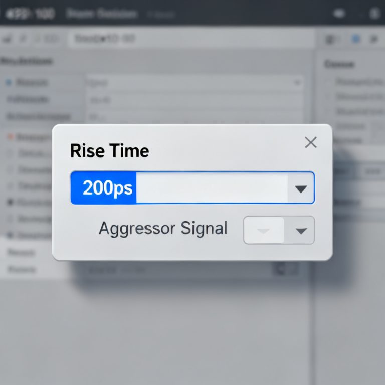
Impedance Control PCB for PCIe 5.0 must be verified using TDR. This method sends a fast pulse down the trace and measures reflections. Use a dedicated test coupon on the panel edge. Acceptance criteria per IPC-2141A include: impedance within ±10% of target, minimal ripple (< 1–2 Ω), and rise time ≤ 35 ps.
VNA (Vector Network Analyzer) – Frequency Domain Analysis
A VNA measures S-parameters for insertion loss, return loss, and crosstalk. For PCIe 5.0 compliance, return loss should be < -15 dB up to 16 GHz. Use VNA for final compliance testing or characterization of critical channels.
Microsectioning – Physical Verification
This destructive test examines trace width, spacing, and dielectric thickness under a microscope. It validates TDR results and diagnoses manufacturing issues like under-etching or resin starvation.
IPC-TM-650 Method 2.5.5.7
This formal standard specifies coupon design and measurement procedures. Ensure your manufacturer provides a test report with target impedance, measured values, TDR trace, and pass/fail status.
Common Pitfalls and How to Avoid Them
Ignoring the Reference Plane Return Path
A discontinuous ground plane causes impedance spikes. Always route PCIe 5.0 traces over a solid, continuous ground plane. Avoid vias, splits, or cutouts in this plane.
Using Incorrect Dielectric Constant (Dk)
FR-4 Dk varies with frequency. Use the frequency-dependent Dk at 16 GHz from your laminate supplier. For high-speed designs, consider low-loss materials like Isola I-Tera MT40 or Rogers 4350B.
Overlooking Copper Surface Roughness
At high frequencies, copper roughness increases losses. Use reverse-treated foil (RTF) or very low profile (VLP) copper for outer layers, and specify smooth copper for inner layers.
Incorrect Via Design
Vias introduce discontinuities. Use back-drilling to remove stubs, grounded via stitching, and maintain equal length and spacing for differential vias.
Best Practices for PCIe 5.0 PCB Design
Stackup Design
Use a symmetric stackup (e.g., 10-layer or 12-layer) to prevent warpage. Place high-speed signal layers adjacent to a ground plane. Use thin dielectrics (3–5 mils) and low-loss laminate with Dk ≤ 3.7 at 16 GHz.
Routing Guidelines
Keep traces in a differential pair within ±5 mils of each other. Avoid 90-degree corners; use 45-degree or curved corners. Minimize vias, and keep total trace length under 10 inches (250 mm).
Simulation Before Fabrication
Use 3D EM simulation (e.g., Ansys HFSS) for critical differential pairs and via transitions. Simulate the full channel from driver to receiver, and compare against PCIe 5.0 base specification (e.g., insertion loss < -20 dB at 16 GHz).
Impedance Control Specifications Table
| Parameter | Impedance Control PCB for PCIe 5.0 Target | Tolerance |
|---|---|---|
| Single-Ended Impedance | 50 Ω | ±10% |
| Differential Impedance | 85 Ω | ±10% |
| Trace Width (typical) | 4–8 mils | ±0.5 mil |
| Dielectric Height (typical) | 4–6 mils | ±10% |
| Return Loss at 16 GHz | < -15 dB | Per PCI-SIG |
Comparison: 85 Ω vs 100 Ω Differential Impedance
| Feature | 85 Ω (PCIe 5.0 Standard) | 100 Ω (Legacy) |
|---|---|---|
| Power Consumption | Lower | Higher |
| Jitter Performance | Better at 32 GT/s | Acceptable at 16 GT/s |
| Signal Integrity | Optimized for high speed | Sufficient for older standards |
| Compatibility | PCIe 5.0 native | PCIe 4.0 and earlier |
Frequently Asked Questions
What is the exact impedance requirement for a PCIe 5.0 differential pair?
The differential impedance requirement for an Impedance Control PCB for PCIe 5.0 is 85 Ω ± 10%. This is a reduction from the 100 Ω used in PCIe 4.0 to improve power efficiency and signal integrity at 32 GT/s.
How do I verify impedance on my PCIe 5.0 PCB?
Verification is done using TDR (Time Domain Reflectometry) on a test coupon, following IPC-TM-650 Method 2.5.5.7. The measured impedance must be within ±10% of the target value, and the TDR trace should show minimal ripple.
What materials are best for PCIe 5.0 impedance control?
Low-loss laminates with stable dielectric constant (Dk) at high frequencies, such as Isola I-Tera MT40, Nelco N4000-13, or Rogers 4350B, are recommended. These materials minimize signal loss and maintain consistent impedance up to 16 GHz.
Can I use standard FR-4 for PCIe 5.0?
Standard FR-4 is generally not recommended for PCIe 5.0 due to its variable Dk at high frequencies and higher loss. For reliable Impedance Control PCB for PCIe 5.0, use a low-loss laminate to ensure consistent performance.
What is the tolerance for trace width in impedance control?
The typical tolerance for trace width is ±0.5 mil, but this depends on the manufacturer’s etching process. Tighter tolerances (e.g., ±0.2 mil) may be required for critical high-speed designs and can be achieved with advanced manufacturing techniques.

Glossary of Key Terms
- Impedance Control PCB for PCIe 5.0: The practice of designing and manufacturing a PCB to maintain a specific electrical impedance (50 Ω single-ended, 85 Ω differential) for high-speed signals at 32 GT/s.
- Single-Ended Impedance: The impedance of a single trace measured to a reference plane, typically 50 Ω for PCIe 5.0.
- Differential Impedance: The impedance of a pair of traces carrying complementary signals, specified as 85 Ω for PCIe 5.0.
- TDR (Time Domain Reflectometry): A measurement technique using a fast pulse to detect impedance variations along a trace.
- VNA (Vector Network Analyzer): A device that measures S-parameters to characterize signal behavior in the frequency domain.
- Microsectioning: A destructive test that physically examines trace geometry and dielectric thickness under a microscope.
- Dielectric Constant (Dk): A material property that affects signal propagation speed and impedance; must be accurately known at the operating frequency.