Crosstalk in High Speed PCB designs is a critical signal integrity challenge that directly degrades the eye diagram, reducing both voltage and timing margins. This comprehensive guide explains how to isolate crosstalk effects using advanced simulation techniques, enabling engineers to achieve robust high-speed performance.
Understanding Crosstalk in High Speed PCB Interconnects
What is Crosstalk?
Crosstalk in High Speed PCB systems is the unwanted electromagnetic coupling between adjacent signal traces, vias, or components. It arises from two fundamental mechanisms:
- Capacitive Coupling (Electric Field): Occurs when the electric field from an aggressor trace induces a voltage on a victim trace. This is dominant in high-impedance circuits and closely spaced traces.
- Inductive Coupling (Magnetic Field): Arises from mutual inductance, where a changing current in the aggressor induces a voltage in the victim. This is dominant in low-impedance circuits and at high frequencies.
Key Types of Crosstalk
- Near-End Crosstalk (NEXT): Measured at the end of the victim line closest to the aggressor driver. It manifests as a positive pulse (if both lines are driven in the same direction) or negative pulse (if opposite).
- Far-End Crosstalk (FEXT): Measured at the far end of the victim line. FEXT is typically a delayed, often larger pulse that arrives after the main signal, causing timing jitter.
Crosstalk in High-Speed Digital Systems
At high speeds (e.g., >1 Gbps), even small crosstalk voltages can corrupt the signal. The effects include:
- Increased Jitter: Crosstalk-induced noise shifts the zero-crossing point of the victim signal, leading to timing uncertainty.
- Reduced Voltage Margin: The eye opening (both vertical and horizontal) shrinks, making it harder for the receiver to distinguish logic 1 from logic 0.
- Pattern-Dependent Errors: Crosstalk amplitude often varies with the data pattern on the aggressor line, leading to deterministic jitter (DJ) that is not random.
The Eye Diagram as a Diagnostic Tool for Crosstalk in High Speed PCB
What is an Eye Diagram?
An eye diagram is an oscilloscope display of a digital signal repeatedly sampled over a unit interval (UI). It overlays many bit periods to reveal:
- Eye Height: Voltage margin (difference between high and low levels minus noise).
- Eye Width: Timing margin (the time during which the signal is valid).
- Jitter: Horizontal spread at the crossing points.
- Noise: Vertical spread in the eye opening.
How Crosstalk Appears in an Eye Diagram
When crosstalk in High Speed PCB is present, the eye diagram exhibits:
- Vertical Eye Closure: The eye height reduces due to induced voltage noise. This is often seen as a “fuzzy” or “thickened” band at the logic levels.
- Horizontal Eye Closure: The eye width narrows due to jitter from crosstalk-induced timing shifts.
- Asymmetric Distortion: NEXT and FEXT may cause different distortion patterns on the rising and falling edges.
- Ghosting or Double-Edges: In severe cases, FEXT can create false pulses that appear as secondary eyes.
Why Isolating Crosstalk Effects Matters
In a real PCB, multiple factors degrade the eye: insertion loss, reflections, power supply noise, and crosstalk. To design effective mitigation, you must isolate the contribution of crosstalk from other loss mechanisms. This allows you to:
- Determine if crosstalk is the dominant limiter.
- Validate specific design changes (e.g., increasing spacing, adding guard traces).
- Meet specification margins (e.g., for PCIe, USB, or Ethernet).
Simulation Methodology for Crosstalk Isolation in High Speed PCB
Simulation Setup Essentials
To isolate crosstalk in an eye diagram simulation, you must replicate the physical environment accurately. Use a 3D field solver (e.g., Ansys HFSS, CST, or Keysight ADS) or a 2D solver (e.g., Polar Si9000) for transmission line parameters. Key steps:
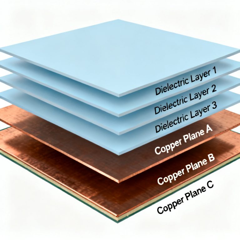
Step 1: Define the Stackup and Geometry
- Specify layer stackup, dielectric material (e.g., FR4, Megtron 6), copper roughness, and trace dimensions.
- Include multiple aggressor and victim traces—typically 3 to 5 lines to capture coupling.
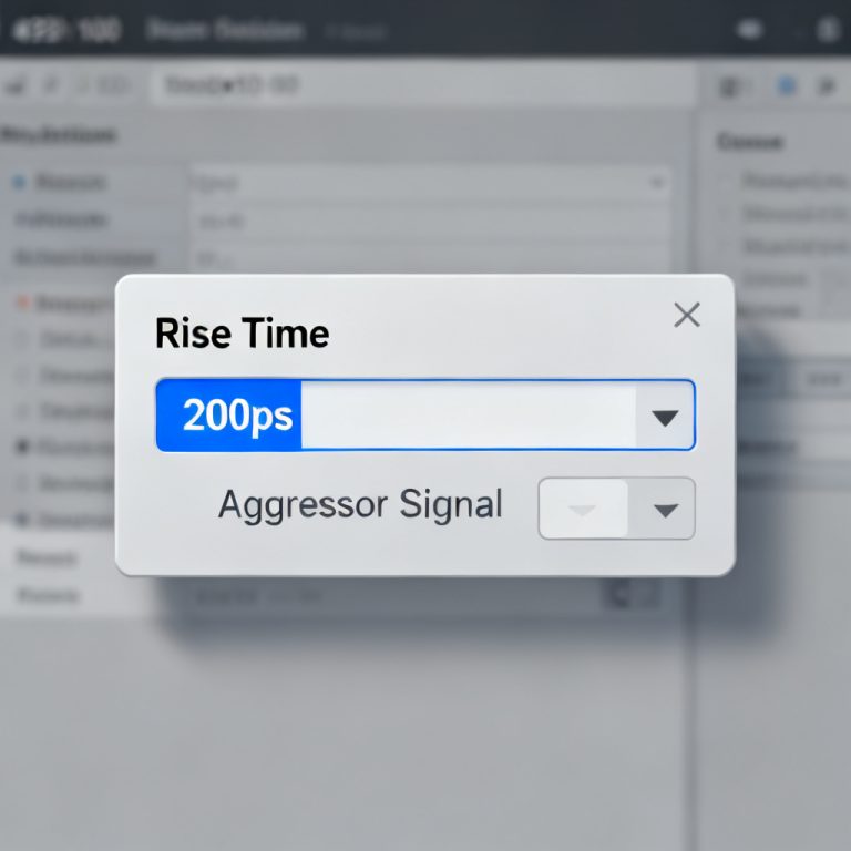
Step 2: Set Up the Stimulus
- Use PRBS (Pseudo-Random Binary Sequence) data patterns (e.g., PRBS7 or PRBS15) to mimic real traffic.
- Drive aggressors with independent or correlated data patterns. For worst-case analysis, use opposite-phase aggressors.
Step 3: Include IBIS Models
- Use IBIS (I/O Buffer Information Specification) models for drivers and receivers. This captures non-linear driver behavior (slew rate, output impedance) that affects crosstalk.
Step 4: Run Transient Simulation
- Simulate for at least 10,000 bits to obtain a statistically significant eye diagram.
- Record time-domain waveforms at the victim receiver.
Isolating Crosstalk: The Baseline Method
The most reliable technique is to compare two simulations:
Simulation A: Full System (Crosstalk Included)
- Simulate all traces as designed. The resulting eye diagram includes all effects: insertion loss, reflections, and crosstalk.
Simulation B: No Crosstalk (Ideal Isolation)
- Modify the simulation to remove coupling. There are three ways:
- Set Mutual Inductance and Capacitance to Zero: In a circuit simulator, zero out the coupling matrices.
- Use Ideal Isolation: Place aggressor traces far apart (e.g., >10x trace width) or remove them entirely.
- Use a Single Trace Simulation: Simulate only the victim line with no neighbors.
Analysis:
- Overlay the eye diagrams from A and B. The difference in eye height, eye width, and jitter is directly attributable to crosstalk.
- For quantitative metrics, measure:
- Vertical Eye Opening (VEO): Compare VEO_A vs VEO_B. The reduction is crosstalk-induced noise.
- Total Jitter (TJ): Compare TJ_A vs TJ_B. The increase is crosstalk-induced jitter.
- Eye Mask Margin: If using a standard eye mask (e.g., PCIe Gen4), check which simulation fails.
Advanced Isolation Techniques
Frequency-Domain Crosstalk Analysis
- Compute S-parameters for the victim and aggressor lines.
- S-parameter Decomposition: Isolate the coupling S-parameters (e.g., S21 for insertion loss, S31 for crosstalk). Convert to time domain via IFFT to see crosstalk impulse response.
- Crosstalk Transfer Function: Plot S31 (FEXT) or S41 (NEXT) magnitude vs frequency. This shows which frequencies contribute most to eye closure.
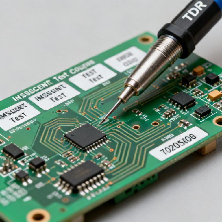
Time-Domain Reflectometry (TDR) with Crosstalk
- Use a TDR simulation to identify impedance discontinuities that exacerbate crosstalk.
- Inject a step pulse into the aggressor and observe the victim TDR response. A spike indicates strong coupling at that location.
Pattern-Dependent Separation
- Simulate with different aggressor patterns (e.g., all 1s, all 0s, alternating 1010). The variation in eye closure reveals crosstalk sensitivity.
- Use Bit Error Rate (BER) Contour analysis: plot the BER as a function of sampling point. Crosstalk creates asymmetric contours.
Practical Techniques to Isolate and Mitigate Crosstalk in High Speed PCB
Physical Design Mitigation
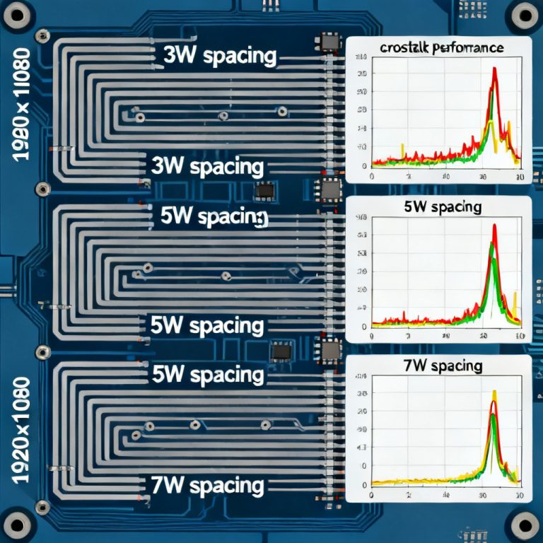
- Increase Trace Spacing: The golden rule is 3W (3x trace width) spacing for moderate crosstalk reduction; 5W for high immunity. Use differential pairs with controlled spacing.
- Guard Traces and Ground Vias: A grounded guard trace between aggressor and victim can reduce coupling by 10-20 dB. Place ground vias at both ends and along the guard trace (every 1/10 wavelength).
- Layer Separation: Route high-speed signals on different layers with a ground plane in between. Stripline (inner layer) offers better isolation than microstrip (outer layer).
- Avoid Parallel Routing: Minimize parallel run lengths. If unavoidable, use serpentine or meandered routing to break coupling.
Simulation-Based Mitigation
- Termination Optimization: Use series or parallel termination to match impedance and reduce reflections that amplify crosstalk.
- Via Stub Removal: Back-drill vias to eliminate stubs that act as resonant antennas for crosstalk.
- Material Selection: Use low-loss dielectrics (e.g., Rogers, Megtron) to reduce dielectric absorption that worsens crosstalk at high frequencies.
Validation with Eye Diagram
After implementing mitigation, re-run the isolation simulation (Simulation B vs A). The goal is to make the eye diagram of the full system (A) approach the ideal (B). Key metrics:
- Eye Height Improvement: Target >10% increase.
- Jitter Reduction: Target >5% decrease in TJ.
- Eye Mask Pass: Ensure the eye mask margin (e.g., 20% margin) is achieved.
Case Study: Isolating Crosstalk in a 10 Gbps Serial Link
Problem Setup
- 4-layer PCB, FR4, 10 Gbps NRZ signaling.
- Victim trace: 6 inches long, 50-ohm microstrip.
- Two aggressor traces: 0.5 mm spacing (2W), 8 inches long.
- Simulation tools: Keysight ADS with 3D EM solver.
Baseline Simulation
- Full System: Eye height = 350 mV, Eye width = 0.85 UI, TJ = 0.12 UI.
- No Crosstalk: Eye height = 450 mV, Eye width = 0.92 UI, TJ = 0.07 UI.
- Isolated Crosstalk Effect: Eye height reduction = 100 mV (22%), Jitter increase = 0.05 UI (71% of total jitter).
Mitigation Steps
- Increase spacing to 3W (0.75 mm) → Eye height improves to 400 mV.
- Add guard trace with ground vias every 5 mm → Eye height improves to 430 mV.
- Use stripline routing on inner layer → Eye height reaches 440 mV.
Final Validation
- Full system eye height = 440 mV (close to ideal 450 mV).
- TJ = 0.08 UI (only 0.01 UI above ideal).
- Result: Crosstalk is no longer the dominant limiter; insertion loss now dominates.
Advanced Topics and Common Pitfalls in Crosstalk in High Speed PCB
Pitfall: Ignoring Power Distribution Network (PDN) Crosstalk
Crosstalk is not limited to signal traces. Power plane coupling can inject noise into the eye. Always include PDN models in your simulation.
Pitfall: Using Only 2D Solvers
2D solvers neglect 3D effects like via coupling and trace bends. For accurate crosstalk isolation, use 3D EM simulation for critical sections.
Pitfall: Overlooking Differential Crosstalk
In differential pairs, common-mode crosstalk can convert to differential noise. Use mixed-mode S-parameters (SDD21, SCC21) to isolate.
Advanced: Machine Learning for Crosstalk Prediction
Recent research uses neural networks to predict crosstalk-induced eye closure from layout parameters. This speeds up design space exploration.
Comparison Table: Key Parameters for Crosstalk in High Speed PCB
| Parameter | High Speed PCB Crosstalk Impact | Recommended Value |
|---|---|---|
| Trace Spacing | Reduces capacitive and inductive coupling | 3W to 5W |
| Guard Trace Width | Provides shielding between traces | At least 1.5x trace width |
| Layer Type | Stripline offers better isolation than microstrip | Stripline for critical nets |
| Dielectric Material | Low Dk/Df reduces signal loss and coupling | Rogers, Megtron 6 |
| Via Stub Length | Resonant stubs amplify crosstalk | < 1/10 wavelength |
Industry Terminology Explained
- Aggressor vs Victim Nets Crosstalk: The net that induces noise is the aggressor; the net that receives noise is the victim.
- 3W Rule Crosstalk High Speed PCB: A design guideline where trace spacing is three times the trace width to minimize coupling.
- Differential Pair Crosstalk High Speed PCB: Crosstalk that affects differential pairs, often converting common-mode noise to differential noise.
- Microstrip vs Stripline Crosstalk Comparison: Microstrip has higher crosstalk due to exposed fields; stripline has lower crosstalk due to shielding by ground planes.
- Via Stub Crosstalk Effect: Unused via stubs act as resonant structures that can amplify crosstalk at specific frequencies.
FAQ: Crosstalk in High Speed PCB Eye Diagram Simulation
Q1: What is the primary cause of crosstalk in High Speed PCB designs?
A1: The primary cause of crosstalk in High Speed PCB designs is electromagnetic coupling between adjacent traces, vias, or components, driven by capacitive and inductive fields.
Q2: How does crosstalk affect the eye diagram in high-speed simulations?
A2: Crosstalk in High Speed PCB simulations reduces eye height and eye width, increases jitter, and can cause asymmetric distortion or ghosting in the eye diagram.
Q3: What is the best method to isolate crosstalk effects in simulation?
A3: The best method is the baseline comparison: simulate the full system (with crosstalk) and an ideal system (without crosstalk by removing coupling), then compare eye diagram metrics.
Q4: Can guard traces completely eliminate crosstalk in High Speed PCB?
A4: Guard traces can significantly reduce crosstalk (by 10-20 dB) but cannot completely eliminate it. Proper grounding via stitching is essential for effectiveness.
Q5: Why is stripline preferred over microstrip for reducing crosstalk?
A5: Stripline routing places traces between ground planes, providing natural shielding that reduces both NEXT and FEXT compared to microstrip, which has exposed fields.
Conclusion: Mastering Crosstalk Isolation
Crosstalk in High Speed PCB designs is a manageable challenge when approached systematically. By combining rigorous simulation with the isolation techniques outlined—baseline comparisons, frequency-domain analysis, and pattern-dependent separation—you can pinpoint crosstalk’s exact contribution to eye diagram degradation. With this knowledge, you can implement targeted physical design improvements (spacing, guard traces, layer selection) and validate them through iterative simulation. The result is a robust, high-speed PCB that meets stringent signal integrity requirements, ensuring reliable data transmission in your products.
For your next high-speed project, remember: isolate first, then mitigate. This approach saves time, reduces costs, and delivers first-pass design success.
Need a partner for your high-speed PCB manufacturing? We specialize in high-speed PCBs with controlled impedance, advanced materials, and SI simulation support. Contact us for a quote or design review.