In high-speed PCB design, mastering how to use Smith Chart to analyze reflection in transmission line is essential for signal integrity. This guide synthesizes expert knowledge to provide a complete, actionable understanding of reflection analysis, specifically for B2B PCB engineers and designers.

Fundamentals: How to Use Smith Chart to Analyze Reflection in Transmission Line
1.1 What is Reflection in a Transmission Line?
Reflection occurs when a signal traveling along a transmission line encounters an impedance discontinuity (e.g., at a load, via, or connector). The ratio of the reflected voltage to the incident voltage is the reflection coefficient (Γ). It is a complex number (magnitude and phase) defined as:
Γ = (Z_L – Z_0) / (Z_L + Z_0)
Where Z_L is the load impedance and Z_0 is the characteristic impedance of the transmission line (typically 50Ω or 75Ω in PCB designs). A perfect match (Z_L = Z_0) yields Γ = 0 (no reflection). An open or short circuit yields |Γ| = 1 (total reflection).
1.2 Why the Smith Chart?
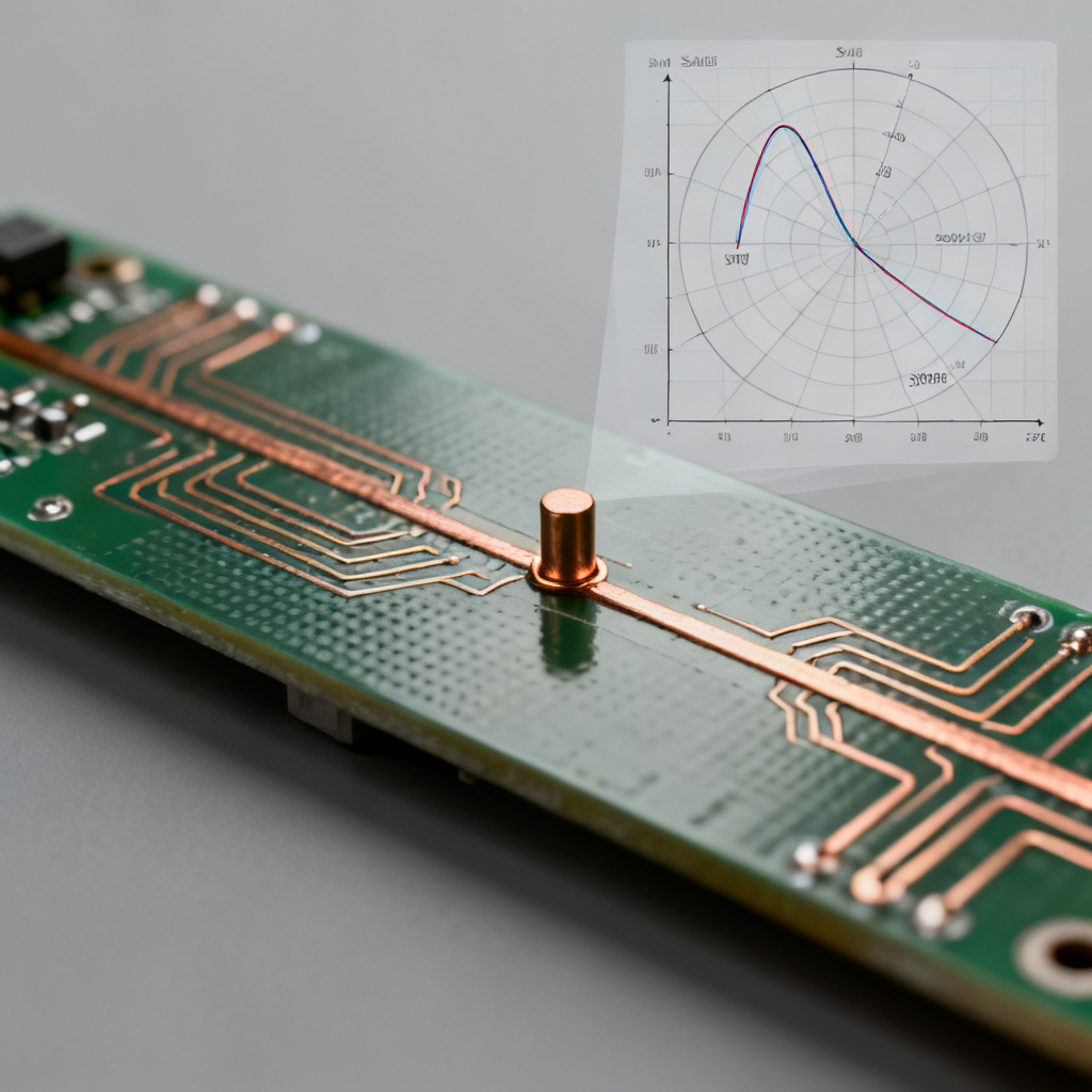
The Smith Chart is a polar plot of the reflection coefficient overlaid with constant resistance and reactance circles. It provides a visual, intuitive way to:
- Convert between impedance and reflection coefficient.
- Perform impedance matching without complex algebra.
- Visualize how impedance changes along a transmission line.
- Analyze VSWR, return loss, and input impedance.
1.3 Key Parameters on the Smith Chart
- Center Point (1,0): Represents Z = Z_0 (perfect match, Γ = 0).
- Outer Circle: Represents |Γ| = 1 (pure reactance or open/short).
- Constant Resistance Circles: Vertical circles intersecting the real axis (e.g., R=0, R=1, R=∞).
- Constant Reactance Arcs: Curves above (inductive, +jX) and below (capacitive, -jX) the real axis.
- Wavelength Scale: Around the perimeter, in fractions of wavelength (λ) toward generator (clockwise) or toward load (counterclockwise).
Step-by-Step: How to Use Smith Chart to Analyze Reflection in Transmission Line

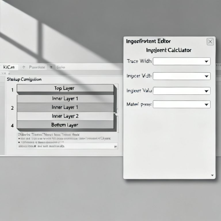
2.1 Step 1: Normalize the Load Impedance
To use the Smith Chart, you must first normalize the load impedance relative to the system’s characteristic impedance (Z_0).
Formula: z_L = Z_L / Z_0
Example: If Z_L = 100 + j50 Ω and Z_0 = 50 Ω, then z_L = 2 + j1.0. Plot this normalized impedance on the chart by finding the intersection of the constant resistance circle R=2 and the constant reactance arc X=+1.0 (inductive). This point represents the load’s reflection coefficient magnitude and phase.
2.2 Step 2: Determine the Reflection Coefficient (Γ)
The distance from the center of the Smith Chart to the plotted load point is proportional to |Γ|. The angle from the positive real axis (clockwise) gives the phase angle.
- Magnitude: Measure the distance from center to point. For example, a point at z=2+j1 has |Γ| ≈ 0.45.
- Phase: Read the angle on the outer circle. For z=2+j1, the phase is approximately 26.6°.
- Equation: Γ = |Γ| * e^(jθ)
2.3 Step 3: Calculate VSWR (Voltage Standing Wave Ratio)
VSWR quantifies the impedance mismatch. It is a real number ≥ 1, where 1 is perfect match.
- Method 1 (from Γ): VSWR = (1 + |Γ|) / (1 – |Γ|)
- Method 2 (from Smith Chart): Draw a circle centered at the chart center through the load point. Where this circle intersects the positive real axis (right side), read the VSWR value. For |Γ|=0.45, VSWR ≈ 2.6.
2.4 Step 4: Find Input Impedance at Any Point on the Line
As you move along a transmission line, the impedance rotates around the Smith Chart at a constant radius (constant |Γ|). The rotation is proportional to the electrical length (in wavelengths) of the line.
- Toward Generator (Source): Rotate clockwise on the chart.
- Toward Load: Rotate counterclockwise.
- Wavelength Scale: The outer circle has a scale in λ. One full rotation (360°) equals 0.5λ.
- Example: If the line is 0.1λ long from the load to the generator, rotate the load point clockwise by 0.1λ (72°). The new point gives the input impedance (Z_in) seen at the generator end.
2.5 Step 5: Analyze Return Loss and Power Transfer
- Return Loss (RL): RL (dB) = -20 * log10(|Γ|). A higher RL indicates better match (e.g., RL=20dB means only 1% power reflected).
- Power Delivered: P_delivered = P_incident * (1 – |Γ|^2). For |Γ|=0.45, only ~80% of power is delivered.
Practical Applications: How to Use Smith Chart to Analyze Reflection in Transmission Line for High-Speed PCB
3.1 Impedance Matching Using Stubs
Stubs (open or shorted transmission line segments) are common in PCB layouts for matching. On the Smith Chart:
- Open Stub: Starts at the open circuit point (rightmost point, R=∞, X=0). Rotating clockwise adds inductive reactance; counterclockwise adds capacitive.
- Shorted Stub: Starts at the short circuit point (leftmost point, R=0, X=0). Rotating clockwise adds capacitive reactance; counterclockwise adds inductive.
- Matching Procedure: Plot the load impedance. Use the chart to find a stub length and position that cancels the reactive component and transforms the impedance to Z_0.
3.2 Single-Stub Matching Example
Problem: Match Z_L = 100 + j50 Ω to a 50Ω line at 2.4 GHz.
- Normalize: z_L = 2 + j1.
- Plot on Smith Chart. Find the constant |Γ| circle.
- Rotate clockwise along the circle until you intersect the constant conductance circle g=1 (the unity circle).
- Read the distance (in λ) from load to that intersection: e.g., 0.162λ.
- At that point, the normalized admittance y = 1 + jB. To cancel the susceptance, add a stub with susceptance = -jB.
- For a shorted stub, start at short circuit and rotate clockwise until you reach the desired susceptance value. Read the stub length: e.g., 0.119λ.
- Result: Place a 0.119λ shorted stub at a distance of 0.162λ from the load.
3.3 Analyzing Reflection in High-Speed Digital Signals
High-speed signals (e.g., DDR, PCIe, Ethernet) are sensitive to even small reflections. The Smith Chart helps:
- Identify problematic impedance discontinuities (e.g., via stubs, connector transitions).
- Design impedance-controlled traces (e.g., microstrip, stripline) to maintain Z_0.
- Evaluate the effect of parasitic capacitance/inductance at component pads (e.g., from SMD resistors or capacitors).
3.4 Using the Smith Chart in Simulation Tools
Modern PCB design software (e.g., Keysight ADS, Ansys HFSS, Altium) integrates Smith Chart functionality for:
- S-parameter analysis: Visualize S11 (input reflection) on the chart.
- Tuning: Adjust component values interactively while watching the impedance path.
- Optimization: Automatically find matching networks for broadband performance.
| Parameter | Smith Chart Symbol | Relevance to Reflection |
|---|---|---|
| Reflection Coefficient (Γ) | |Γ|∠θ | Directly plotted; magnitude indicates mismatch severity |
| VSWR | Read from real axis | Quantifies standing wave ratio; 1 = perfect match |
| Return Loss (dB) | -20 log|Γ| | Higher value = less reflected power |
| Normalized Impedance | z = R + jX | Base for all calculations on chart |
Advanced Techniques: How to Use Smith Chart to Analyze Reflection in Transmission Line
4.1 Dealing with Complex Loads
For loads with significant reactive components (e.g., antenna impedance, transistor input impedance), the Smith Chart simplifies the transformation to a real impedance. Use multiple stubs or lumped elements (capacitors/inductors) in sequence.
4.2 Broadband Matching
Narrowband matching (single frequency) is straightforward. For broadband (e.g., 1-10 GHz), use:
- Multi-section quarter-wave transformers (visualized as multiple rotations on the chart).
- Tapered lines (e.g., Klopfenstein taper).
- Single-stub or double-stub matching with frequency sweeps.
4.3 Common Mistakes
- Forgetting Normalization: Always normalize to Z_0 before plotting.
- Mixing Impedance and Admittance: Remember that rotation on the Smith Chart corresponds to impedance transformation; admittance charts (inverted) are available for shunt elements.
- Ignoring Loss: Real transmission lines have attenuation, which reduces |Γ| over distance. The Smith Chart points spiral inward toward center for lossy lines.
- Incorrect Wavelength Scale: The chart’s wavelength scale is in electrical length (λ), not physical length. For a specific frequency, convert physical length to electrical length using the phase velocity.

Integrating Smith Chart Analysis into Your PCB Workflow
5.1 When to Use the Smith Chart
- Design Phase: To select matching components (stubs, L-C networks) for RF or high-speed digital interfaces.
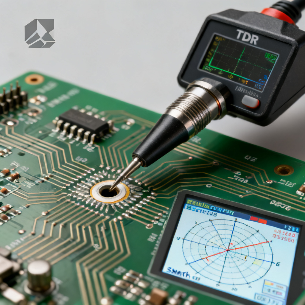
- Debugging Phase: To troubleshoot signal integrity issues (e.g., excessive jitter, ringing) by measuring impedance with a TDR and interpreting results on the chart.
- Verification Phase: To compare simulated vs. measured S-parameters (e.g., from a vector network analyzer) and ensure design meets specifications.
5.2 Tools for Practical Use
- Paper Smith Chart: For quick, manual calculations.
- Software Smith Chart: In tools like Smith Chart Tool (free online), RFSim99, or built-in calculators in PCB layout software.
- Python/MATLAB: For automated analysis of large datasets (e.g., frequency sweeps of S-parameters).
5.3 Case Study: High-Speed PCB Reflection Analysis
Scenario: A 50Ω microstrip line on a 4-layer PCB with a 0.5mm via stub.
- Measure impedance at the via using TDR. Plot on Smith Chart: shows a capacitive dip (negative reactance).
- Rotate toward generator to find the effective impedance at the driver.
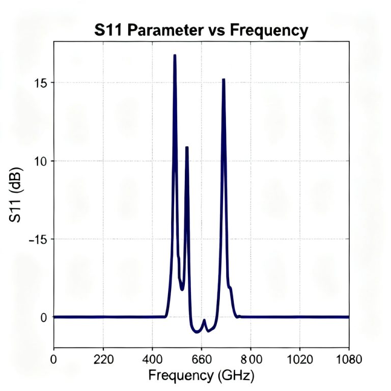
- Design a matching stub (e.g., a small series inductor or a grounded coplanar waveguide) to cancel the capacitance.
- Verify with simulation: S11 improves from -10 dB to -25 dB.
FAQ: How to Use Smith Chart to Analyze Reflection in Transmission Line
What is the primary use of the Smith Chart in PCB design?
The Smith Chart is primarily used to visualize and solve impedance matching problems, calculate reflection coefficient, VSWR, and return loss in transmission lines, which is critical for high-speed PCB design.
How do I plot a load impedance on the Smith Chart?
First normalize the load impedance by dividing by the characteristic impedance (Z_0). Then locate the intersection of the constant resistance circle and constant reactance arc corresponding to the normalized value.
What does a point at the center of the Smith Chart represent?
The center point (1,0) represents a perfect impedance match where Z_L = Z_0, resulting in zero reflection (Γ = 0) and VSWR = 1.
Can the Smith Chart be used for broadband matching?
Yes, but it requires iterative techniques such as multi-section transformers or tapered lines. The chart helps visualize how impedance changes with frequency.
What is the difference between impedance and admittance on the Smith Chart?
Impedance is typically plotted directly. For shunt elements, an admittance chart (inverted) is used, which is the same chart but rotated 180 degrees.