In high-speed PCB design, mastering the return path PCB design is critical for signal integrity. Choosing the correct signal layer vs return layer adjacency directly determines loop inductance, EMI, and overall performance. This guide synthesizes expert insights to help you make the right choice.
Fundamentals of Return Path PCB Design and Plane Adjacency
The return path PCB design relies on physics: at high frequencies, return current follows the path of least inductance, not least resistance. This path is directly beneath the signal trace on the adjacent reference plane.
Inductance Reduction via Proximity in Return Path PCB Design
Closer adjacency between signal layer and return plane reduces loop area and loop inductance. Lower inductance prevents voltage drops and signal reflections, making return path PCB design a top priority for high-speed signals.
Microstrip and Stripline Configurations for Return Path
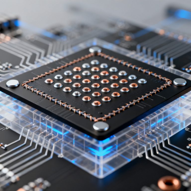
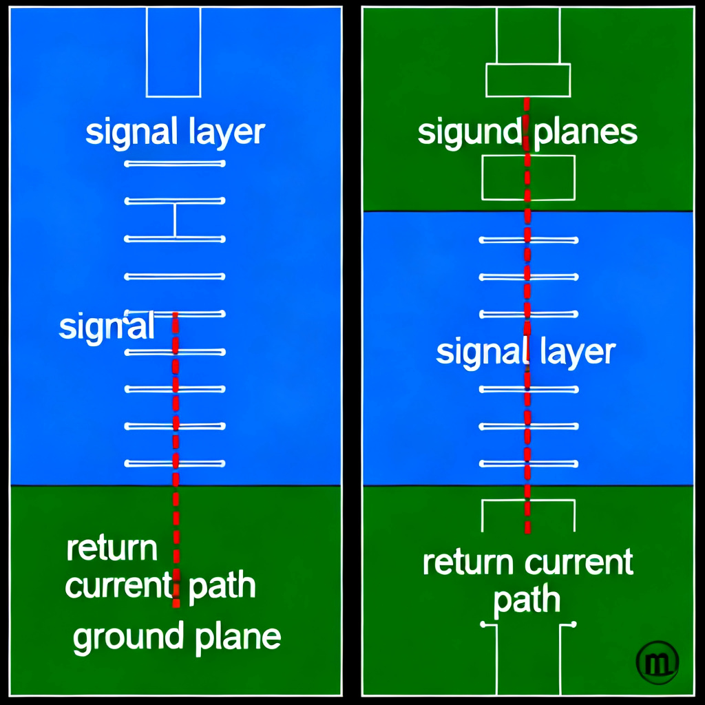
Microstrip places the signal on an outer layer adjacent to a plane—simple but EMI-prone. Stripline sandwiches the signal between two planes for superior shielding. Both rely on tight adjacency for effective return path PCB design.
Rule of Thumb for Adjacency in Return Path PCB Design
For signals above 100 MHz or with fast rise times under 1 ns, the signal layer must be directly adjacent to a solid ground plane. If using a power plane, pair it with a ground plane at less than 5 mils spacing to maintain coupling.
The Danger of Skip Layers in Return Path PCB Design
Avoid placing a signal layer on Layer 3 when the reference plane is on Layer 1 with Layer 2 as a different signal or power plane. This creates large loop areas and unpredictable return paths, violating good return path PCB design.
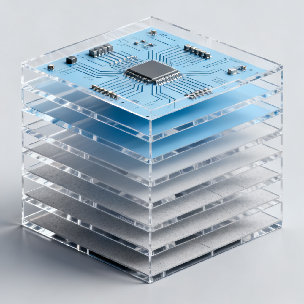
Practical Stackup Design for Optimal Return Path PCB Design
Effective return path PCB design requires planning stackup symmetry from the start. A 6-layer stackup like Signal-Ground-Signal-Power-Ground-Signal ensures every signal layer has an adjacent ground plane.
Choosing Ground vs Power as Return Plane in Return Path PCB Design
Ground is preferred for return path PCB design because it provides a clean, low-impedance 0V reference. Power planes can serve as return planes only if AC-coupled to ground via decoupling capacitors and spaced 3-5 mils from a ground plane.
Layer Pairing Strategy for Return Path PCB Design
Explicitly pair signal layers with their reference planes in your PCB software. For example: Top Layer (Signal) → Layer 2 (Ground Plane); Layer 3 (Signal) → Layer 4 (Ground Plane). Never pair a signal layer with a plane two or more layers away.
Controlled Impedance and Adjacency in Return Path PCB Design
Characteristic impedance (e.g., 50Ω) depends on the distance (H) between signal trace and reference plane. A smaller H allows narrower traces for higher density but increases capacitance. This trade-off must be managed in return path PCB design.
Advanced Considerations for Return Path PCB Design and EMI Control
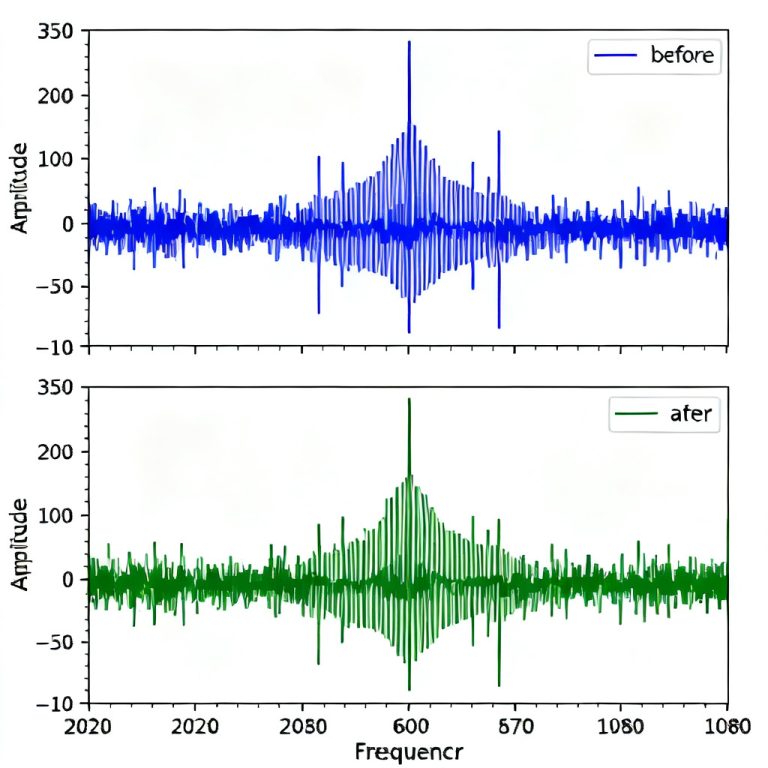
Advanced return path PCB design addresses via transitions, split planes, and discontinuities that cause EMI. These factors can make or break high-speed signal integrity.
The Return Path Discontinuity Problem
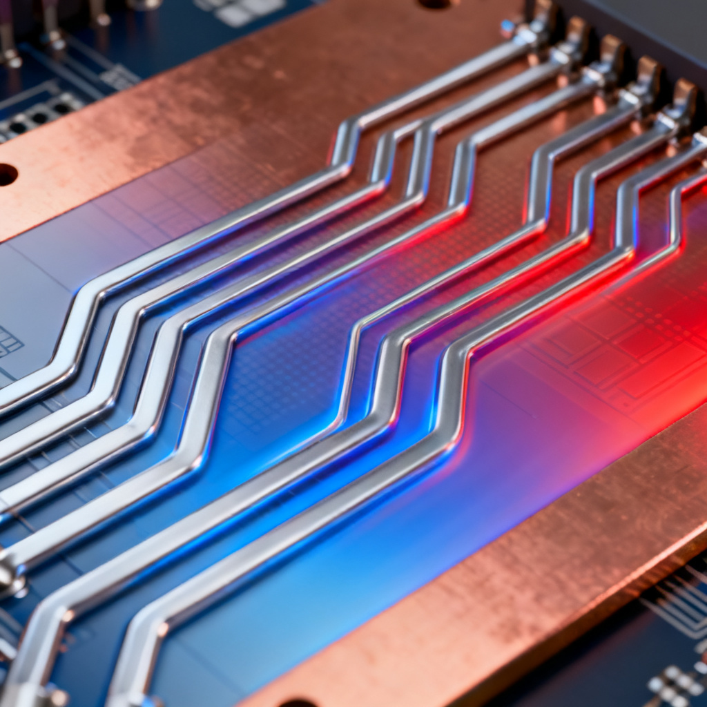
When a signal changes layers, the return current must also change planes. Without low-inductance connections (stitching vias), a large loop antenna forms, radiating EMI. Place a stitching via within 40-60 mils of the signal via to maintain return path PCB design integrity.
Split Planes and Adjacency in Return Path PCB Design
Never route a high-speed signal over a split in its reference plane. The return current will go around the split, creating a large loop. Keep the plane continuous under the signal, or use a ground bridge to preserve return path PCB design.
The Image Plane Concept
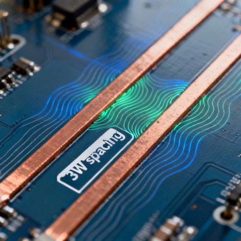
The adjacent plane acts as an image of the signal trace. Use a solid copper pour extending at least 3-5 times the trace width beyond the signal on all sides. This ensures a clean, low-inductance return path PCB design.
Differential Pairs and Adjacency in Return Path PCB Design
For differential signals, the return path is primarily through the other signal in the pair, but a reference plane is still needed for common-mode noise rejection. Route differential pairs over a continuous ground plane with consistent spacing and close adjacency.
Step-by-Step Decision Framework for Return Path PCB Design
Combine all insights into a practical framework for return path PCB design.
Step 1: Classify Your Signals for Return Path PCB Design
High-speed signals (>100 MHz, rise time <1 ns) require mandatory adjacency to a ground plane (e.g., DDR, PCIe). Medium-speed signals (10-100 MHz) highly recommend adjacency. Low-speed signals (<10 MHz) benefit from adjacency but are less critical.
Step 2: Choose Your Stackup for Return Path PCB Design
4-layer board: Signal-Ground-Power-Signal—route high-speed on top layer only. 6-layer board (recommended): Signal-Ground-Signal-Power-Ground-Signal—every signal layer has an adjacent ground plane. 8+ layers: add more ground planes.
Step 3: Verify Plane Continuity in Return Path PCB Design
Ensure the reference plane is solid (no splits, slots, or large cutouts) under the entire high-speed trace. If using a power plane, verify AC-coupling to ground with decoupling capacitors every 1/10th of the signal wavelength. Add stitching vias at via transitions.
Step 4: Control Dielectric Thickness for Return Path PCB Design
Specify dielectric material (e.g., FR-4, Rogers) and thickness between signal layer and reference plane. Thinner dielectrics (4-5 mils) provide tighter coupling and lower inductance. Thicker dielectrics (8-10 mils) reduce capacitance but increase loop inductance.
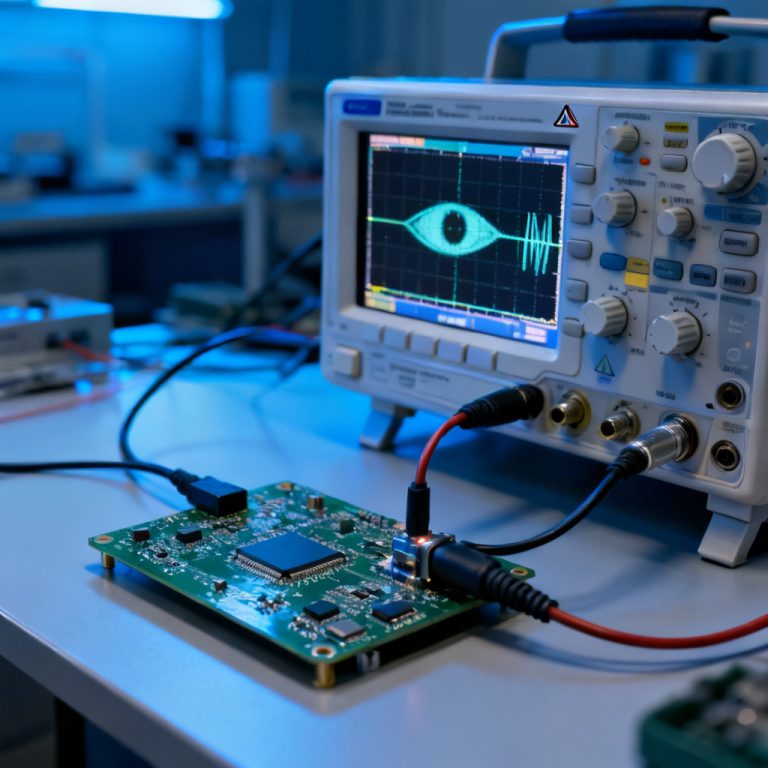
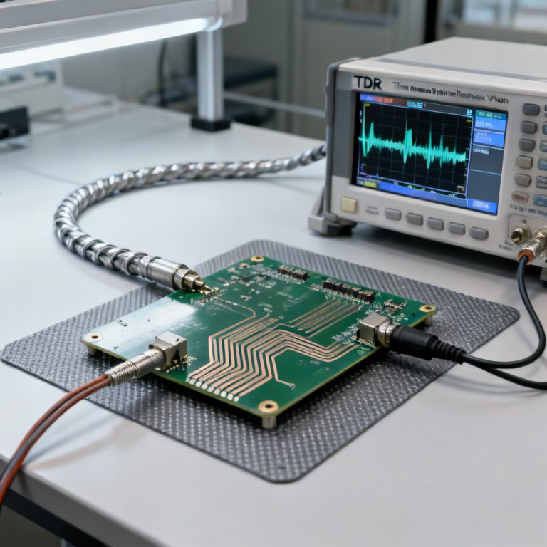
Step 5: Validate with Simulation for Return Path PCB Design
Use field solvers (e.g., HyperLynx, ADS, Saturn PCB Toolkit) to calculate impedance and loop inductance. Simulate return path discontinuities to identify potential EMI hotspots.
Comparison: Our High-Speed PCB Manufacturing vs Standard Approaches
| Parameter | Our Return Path PCB Design Approach | Standard Approach |
|---|---|---|
| Layer Adjacency | Mandatory ground plane adjacency for all high-speed signals | Often uses skip layers or power planes without tight coupling |
| Dielectric Thickness | 4-5 mils for tight coupling and low inductance | 8-10 mils typical, increasing loop area |
| Via Transition Management | Stitching vias placed within 40-60 mils of signal vias | Often omitted, leading to EMI |
| Plane Continuity | Solid copper pours with 3-5x trace width extension | Frequent splits or hatched patterns |
| Impedance Control Tolerance | ±5% on controlled impedance layers | ±10% or unspecified |
Frequently Asked Questions About Return Path PCB Design
What is return path PCB design?
Return path PCB design is the practice of ensuring that high-frequency return currents have a low-inductance path directly beneath the signal trace, typically through an adjacent ground or power plane.
Why is signal layer vs return layer adjacency important?
Proper adjacency minimizes loop inductance, reduces EMI, and maintains signal integrity. Without it, return path PCB design fails, causing reflections and crosstalk.
Can a power plane be used as a return plane?
Yes, but only if it is AC-coupled to ground with decoupling capacitors and spaced very close (3-5 mils) to a ground plane. Otherwise, ground is preferred for return path PCB design.
What happens if I use skip layers in my stackup?
Skip layers create large loop areas and unpredictable return paths, severely degrading return path PCB design. Always use the immediately adjacent layer as the return.
How do stitching vias help return path PCB design?
Stitching vias connect ground planes at via transitions, providing a short return path for the current. This prevents EMI and maintains return path PCB design integrity.
Glossary of Key Terms in Return Path PCB Design
- Return path: The path that current takes to return to its source after traveling through a signal trace.
- Loop inductance: Inductance formed by the signal trace and its return path; minimized by close adjacency.
- Microstrip: A signal trace on an outer layer with a reference plane on the next inner layer.
- Stripline: A signal trace sandwiched between two reference planes.
- Stitching via: A via that connects two ground planes to provide a low-inductance return path.
- Image plane: The reference plane that acts as an electromagnetic image of the signal trace.