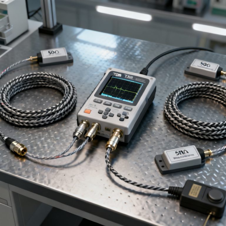
Learn how to use Time Domain Reflectometry (TDR) to identify broken return path PCB design issues. This guide covers TDR theory, setup, waveform analysis, and fixes for high-speed PCB signal integrity.
Understanding the Broken Return Path PCB Design Problem
What Is a Return Path Break?
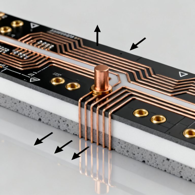
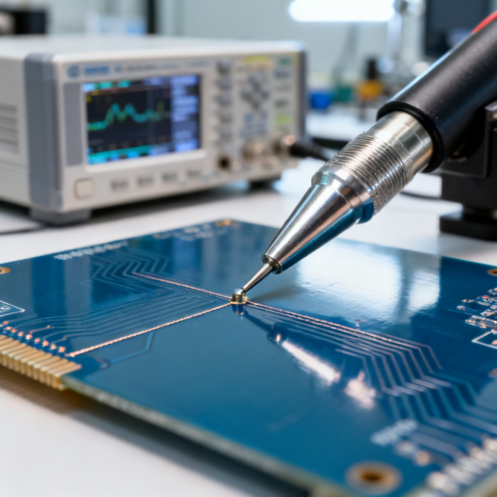
A broken return path PCB design occurs when the continuous copper reference plane beneath a signal trace is interrupted. Common causes include split ground planes, void areas, layer changes without a return via, and slot cuts.
How a Broken Return Path Affects Signal Integrity
When the return current cannot flow directly beneath the signal trace, it creates a broken return path PCB design that causes impedance mismatch, increased crosstalk, common-mode radiation, and rise-time degradation.
Why TDR Is the Ideal Tool
Time Domain Reflectometry (TDR) provides spatial resolution, intuitive waveforms, and works on unterminated or loaded traces, making it ideal for detecting a broken return path PCB design.
TDR Fundamentals for Return Path Detection
TDR Working Principle
A TDR sends a fast step pulse into the transmission line. When the pulse encounters a change in impedance, part of the energy is reflected. The reflection coefficient (Γ) indicates a broken return path PCB design.
Key TDR Parameters for Return Path Analysis
Rise time, time base, impedance scale, and averaging are critical parameters. A faster rise time (e.g., 35 ps) provides higher resolution for detecting a broken return path PCB design.
Interpreting TDR Waveforms
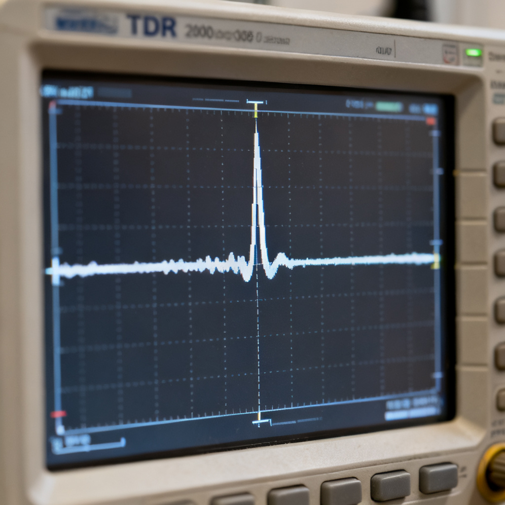
A flat line at Z₀ indicates no discontinuity. A positive spike indicates a broken return path PCB design (higher impedance). A negative dip indicates a short or capacitive discontinuity.
Step-by-Step Procedure to Identify a Broken Return Path PCB Design Using TDR
Step 1: Prepare the PCB and Test Setup
Ensure proper termination, select a test trace, connect the TDR probe, and calibrate. A clean setup is essential for accurately identifying a broken return path PCB design.
Step 2: Set TDR Parameters
Use the fastest rise time (e.g., 35 ps), set the time base to 1.5x the trace length, and reference impedance to 50 Ω. Averaging 16–64 times reduces noise.
Step 3: Capture the TDR Waveform
Launch the measurement. The first impedance change after the launch area indicates the location of a broken return path PCB design.
Step 4: Identify the Broken Return Path Signature
Look for a positive impedance spike not at the trace end. Measure the distance using the formula: Distance = (c × Δt) / (2 × √εr). Compare with layout to pinpoint the broken return path PCB design.
Step 5: Confirm with a Differential Measurement
Use differential TDR to measure odd-mode impedance. An increase in odd-mode impedance confirms a broken return path PCB design.
Common TDR Signatures of Return Path Breaks
Split Ground Plane
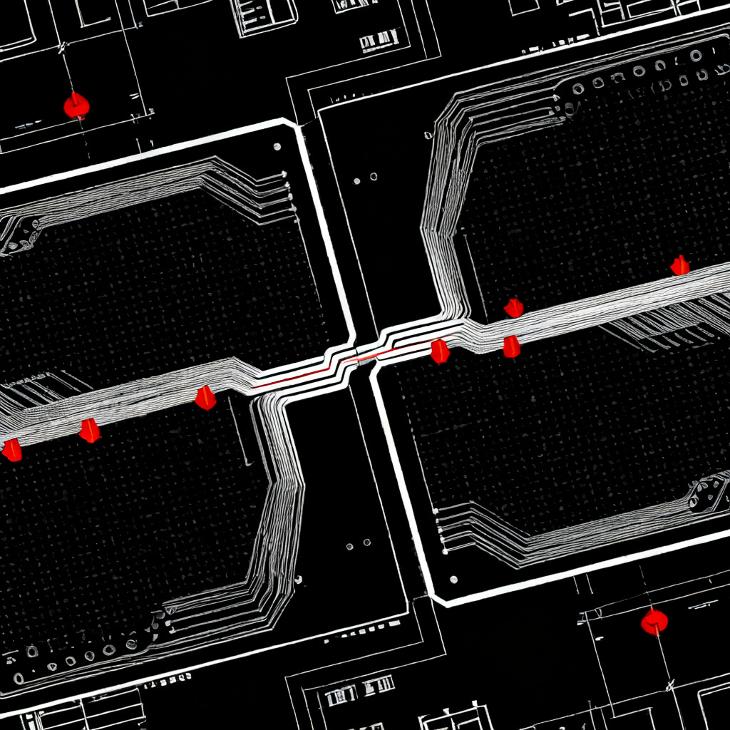
A gradual or stepped increase in impedance over a short distance indicates a broken return path PCB design caused by a split ground plane.
Missing Return Via at Layer Transition
A sharp positive spike exactly at the via location indicates a broken return path PCB design due to a missing return via.
Void Under the Trace
A narrow positive spike with a width equal to the void dimension indicates a broken return path PCB design caused by a void.
Slot or Cutout in Plane
A wide positive spike with multiple reflections indicates a broken return path PCB design caused by a slot or cutout.
How to Fix a Broken Return Path PCB Design Based on TDR Findings
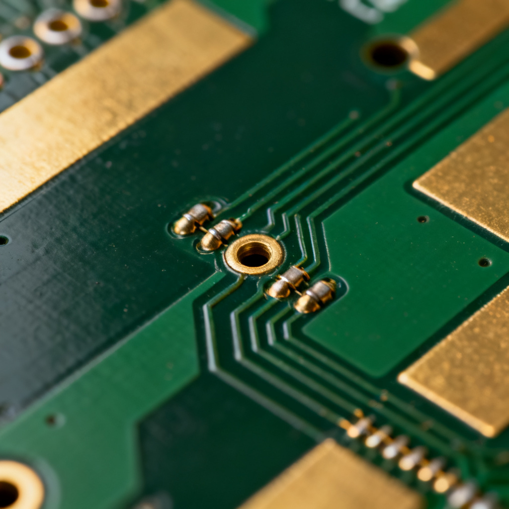
Add Stitching Vias
If the TDR spike occurs at a layer transition, add a ground via within 1 mm of the signal via to fix the broken return path PCB design.
Bridge the Split Plane
Add a copper bridge or capacitor across the split to provide a continuous return path, resolving the broken return path PCB design.
Use a Ground Plane Stitch
Add a ground plane layer directly beneath the trace or fill the void with copper to eliminate the broken return path PCB design.
Optimize Via Stub Length
Back-drill the via or use blind/buried vias to reduce the stub effect, mitigating the broken return path PCB design.
Advanced TDR Techniques for Return Path Analysis
Differential TDR (TDT)
Measure odd-mode impedance of a differential pair. An increase indicates a broken return path PCB design.
Time Domain Transmission (TDT)
Measure the transmitted waveform at the far end. A slower rise time indicates a broken return path PCB design.
3D TDR Mapping
Map impedance in 3 dimensions by measuring multiple launch points, revealing how the broken return path PCB design changes across the board.
Correlation with Simulation
Use a 3D EM simulator to model the broken return path PCB design and compare with measured TDR response.
Troubleshooting Common TDR Measurement Issues
Probe inductance, cable loss, temperature drift, and multiple reflections can affect accuracy. Minimize these to reliably detect a broken return path PCB design.
Case Study – Detecting a Broken Return Path in a 10 Gbps Differential Pair
A 10 Gbps differential pair showed excessive jitter and EMI. TDR revealed a positive spike of 12 Ω at 1.5 ns delay, confirming a broken return path PCB design due to a ground plane split. Adding capacitors and a ground stitch via reduced the spike to < 2 Ω.
Key Parameters for Broken Return Path PCB Design
| Parameter | Value | Impact on Broken Return Path PCB Design |
|---|---|---|
| Rise Time | 35 ps | Higher resolution for detecting broken return path PCB design |
| Impedance Scale | 50 Ω | Standard for high-speed PCB |
| Time Base | 1.5x trace length | Ensures full coverage |
Glossary of Key Terms for Broken Return Path PCB Design
Time Domain Reflectometry (TDR): A measurement technique that sends a fast pulse into a transmission line to detect impedance discontinuities, such as a broken return path PCB design.
Return Path: The path taken by the return current in a PCB. A broken return path PCB design increases loop inductance and causes signal integrity issues.
Impedance Discontinuity: A change in characteristic impedance along a trace, often caused by a broken return path PCB design.
Comparison: TDR vs. VNA for Broken Return Path PCB Design
TDR provides spatial resolution and intuitive waveforms for identifying a broken return path PCB design, while VNA offers frequency-domain analysis. TDR is preferred for locating the exact physical location of the break.
FAQ: Broken Return Path PCB Design Using TDR
What is a broken return path PCB design?
A broken return path PCB design occurs when the continuous copper reference plane beneath a signal trace is interrupted, causing impedance discontinuities and signal integrity problems.
How does TDR help identify a broken return path PCB design?
TDR sends a fast pulse and measures reflections. A positive impedance spike indicates a broken return path PCB design, allowing you to pinpoint its location.
What are common causes of a broken return path PCB design?
Common causes include split ground planes, missing return vias, voids under traces, and slot cuts in the plane.
How can I fix a broken return path PCB design?
Fix it by adding stitching vias, bridging split planes, using ground plane stitches, or optimizing via stub lengths.
Is TDR better than VNA for detecting a broken return path PCB design?
Yes, TDR provides spatial resolution and is more intuitive for locating the exact physical location of a broken return path PCB design.