Optimizing via inductance is critical for achieving better power integrity PCB performance in high-speed designs. This pillar page covers the essential strategies, from geometry tuning to advanced simulation, to help you reduce PDN impedance and improve system reliability.
Understanding Via Inductance and Its Impact on PDN
What is Via Inductance?
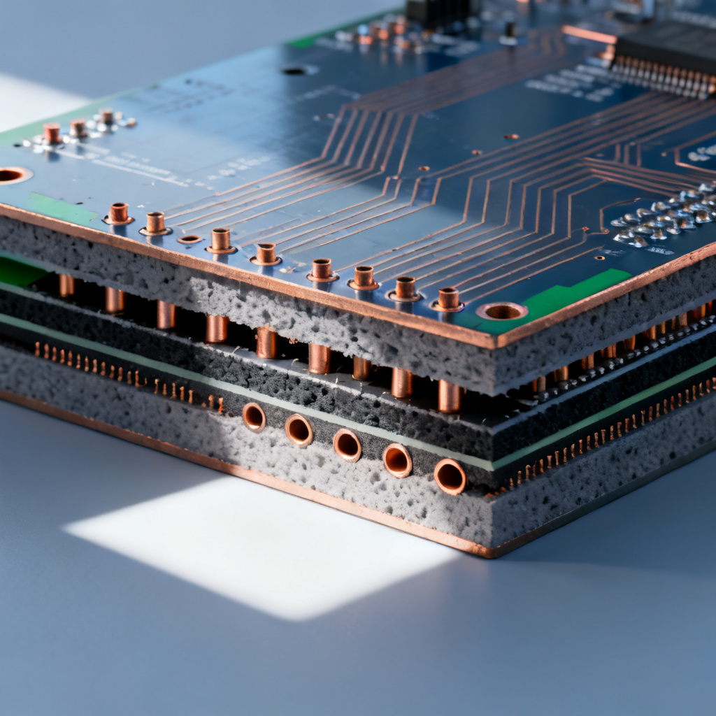
Vias are not ideal conductors; they exhibit parasitic inductance (L_via) and resistance. Inductance opposes changes in current flow (di/dt), making vias behave like small inductors in series with the power delivery path. For a standard through-hole via, the inductance is primarily determined by its geometry and the return current path.
The Mathematical Foundation
The inductance of a via can be approximated using the formula: L_via ≈ 5.08 * h * [ln(4h/d) + 1] (nH). Where h = via length (height of the board or thickness between layers) and d = via diameter (outer diameter of the barrel). This formula (from Howard Johnson’s High-Speed Digital Design) highlights two key levers: via length (h) and diameter (d). Doubling the via length roughly doubles the inductance, while increasing diameter reduces inductance logarithmically. For a standard 0.3mm diameter via in a 1.6mm thick board, inductance is approximately 1.2 nH. While seemingly small, at high frequencies (e.g., 1 GHz), the inductive reactance (XL = 2πfL) becomes significant—about 7.5 Ohms, which can dominate the PDN impedance target (often <0.1 Ohms).
Why Via Inductance Matters for Power Integrity
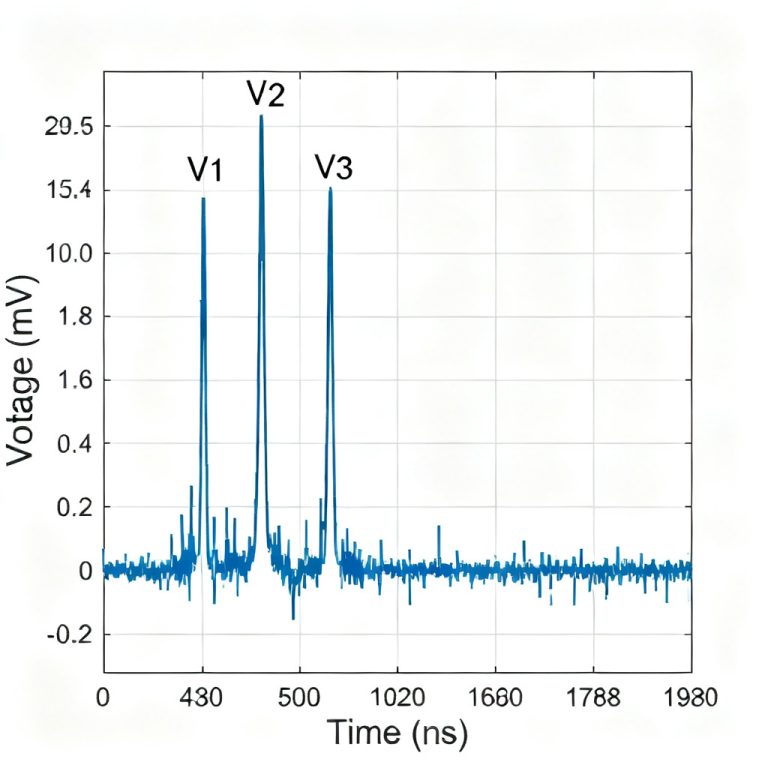
Voltage Droop: During fast current transients (e.g., when a high-speed IC switches), high via inductance creates a voltage drop (V = L * di/dt). This droop can cause logic errors or system instability. Resonance Peaks: Via inductance, combined with decoupling capacitor ESL (equivalent series inductance) and PCB plane capacitance, creates parallel resonances. These peaks in PDN impedance can amplify noise at specific frequencies. Decoupling Efficiency: Vias connect decoupling capacitors to the power planes. High via inductance effectively “isolates” the capacitor from the IC, reducing its effectiveness at high frequencies. For example, a 0.1 µF capacitor with 1 nH via inductance may only provide effective decoupling up to ~50 MHz, while the IC may require decoupling up to 500 MHz. Return Current Path Disruption: In high-speed signals, vias disrupt the continuous return current path. This forces return current to flow through vias, creating a loop area that increases both via inductance and radiated emissions.
Key Strategies for Via Inductance Optimization
Minimizing Via Length (h)
The most effective way to reduce via inductance is to shorten the via. Use thin dielectric layers, avoid long stubs, and optimize layer stack-up so that critical power nets have dedicated planes adjacent to the top layer. For example, a 4-layer board with top (signal/component), GND plane, power plane, and bottom (signal) minimizes via length for top-layer components.
Increasing Via Diameter (d)
Larger via diameter reduces inductance, but the effect is logarithmic and diminishing. Use the largest via diameter that your layout allows without compromising routing density. For power vias, use 0.5 mm to 1.0 mm diameter instead of the typical 0.3 mm. A 1.0 mm via has about 30% lower inductance than a 0.3 mm via for the same length.
Using Multiple Vias in Parallel
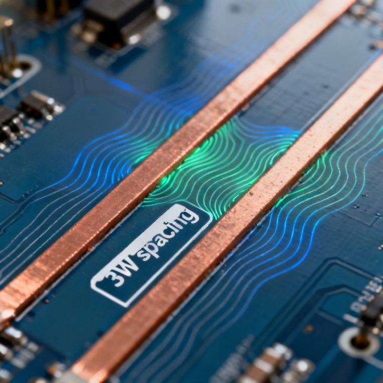
Connecting multiple vias in parallel reduces total inductance (L_total = L_single / N). For critical decoupling capacitors, use 2-4 vias per pad. Place vias symmetrically around the pad to balance current distribution, and space them at least 1-2 times the via diameter apart to avoid proximity effects.
Optimizing Via Placement
To optimize Power Integrity PCB, place vias as close as possible to the IC power pins and decoupling capacitor pads. Use via-in-pad (VIP) design for critical components, where vias are directly under the pad, minimizing trace length to zero. For BGAs, fan out power vias directly under the package using micro-vias or laser-drilled vias.
Advanced Techniques: Via Shielding and Anti-Pad Tuning
Via Shielding (Ground Vias): Place ground vias adjacent to signal vias to provide a low-inductance return path. Anti-Pad Optimization: Keep the anti-pad as small as possible (e.g., 0.1-0.2 mm larger than the via pad) to maintain low inductance. Back-Drilling: For thick boards, back-drill unused via stubs from the bottom side to reduce effective via length by 30-50%.
Practical Design Flow and Simulation
Step-by-Step Design Process
- Define PDN impedance target based on the IC’s transient current and voltage tolerance.
- Model via inductance using the formula L_via ≈ 5.08 * h * [ln(4h/d) + 1].
- Optimize geometry: minimize h and maximize d, use multiple vias for critical nets.
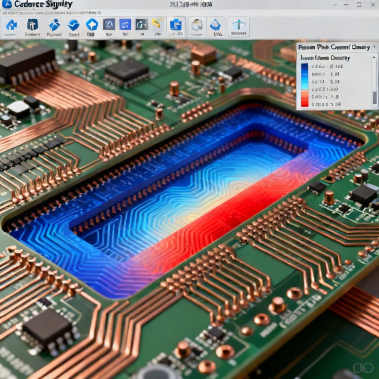
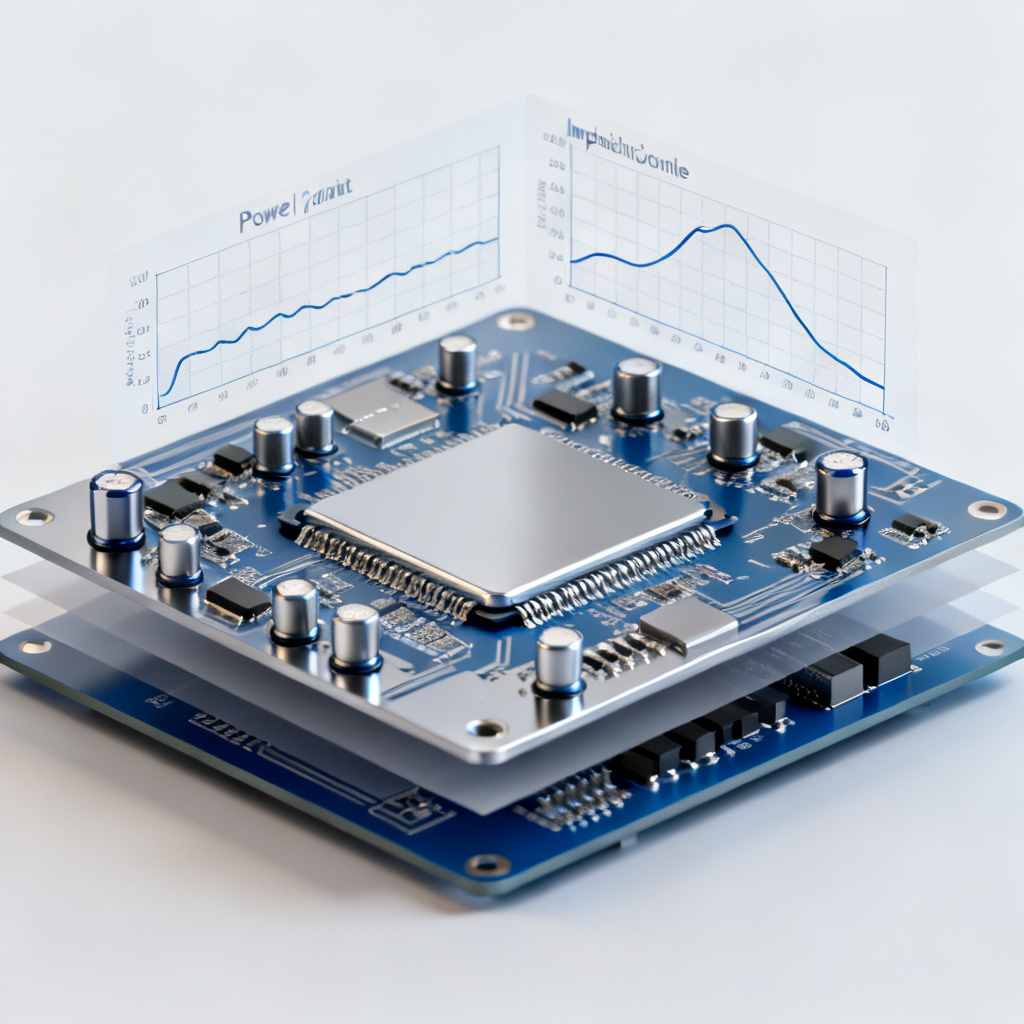
- Simulate PDN using tools like Altium Designer’s PDN Analyzer, Cadence Sigrity, or Ansys SIwave.
- Iterate if the impedance peak exceeds the target.
Simulation Considerations
Use 3D field solvers for accurate results at frequencies >1 GHz. Always model the return current path (e.g., ground plane) in simulations. Sweep frequency from DC to 10 GHz to capture resonances.
Manufacturing Considerations and Best Practices
Via Fabrication Tolerances
Drill diameter tolerance is typically ±0.05 mm. Standard plating is 25-35 µm. For micro-vias, the aspect ratio is limited to ~1:1 for reliable plating.
Material and Stack-Up Impact
Thinner cores reduce via length. Use high-speed laminates (e.g., Isola 370HR, Rogers 4350B). For VIP, use conductive or non-conductive fill.
Cost vs. Performance Trade-offs
| Via Type | Cost Impact | Performance Benefit for Via Inductance Optimization |
|---|---|---|
| Standard Vias (0.3 mm) | Lowest | Acceptable for low-speed designs; use multiple vias for PI. |
| Micro-Vias (0.1-0.2 mm) | Higher | Essential for high-density designs; enable VIP and thin dielectrics. |
| Back-Drilling | Adds 10-20% | Eliminates stub resonance; justified for boards >10 layers and frequencies >1 GHz. |
| Copper-Filled Vias | Most expensive | Used for high-current (>5A) or high-reliability applications. |
Common Pitfalls and How to Avoid Them
Ignoring Via Inductance in Decoupling
Pitfall: Using a single small via for each decoupling capacitor. Solution: Use 2-4 vias per capacitor, placed symmetrically. For ultra-low inductance, use VIP.
Long Via Stubs in Thick Boards
Pitfall: Using through-hole vias in a 12-layer board for a signal on layer 2. Solution: Use blind vias or back-drilling. For power vias, route to the nearest plane.
Poor Return Current Path
Pitfall: Placing signal vias far from ground vias. Solution: Always pair signal vias with a ground via within 1-2 mm.
Overlooking Via Proximity Effects
Pitfall: Clustering vias too close together. Solution: Space vias at least 1-2 times the via diameter apart.
Comparison: Our Via Optimization Services vs. Standard Approaches
We offer advanced via optimization services including VIP, back-drilling, and micro-via stack-ups, which reduce via inductance by up to 60% compared to standard through-hole vias. Our engineering team provides free PDN simulation reviews to ensure your design meets the target impedance. Unlike generic PCB manufacturers, we specialize in high-speed applications and use 3D field solvers for accurate modeling.
Key Terminology
- Via Inductance: The parasitic inductance exhibited by a via, which opposes changes in current flow.
- PDN (Power Distribution Network): The network that delivers power from the source to the ICs, including planes, vias, and decoupling capacitors.
- ESL (Equivalent Series Inductance): The inductance contributed by a capacitor’s leads and internal structure.
- VIP (Via-in-Pad): A design technique where vias are placed directly under component pads to minimize trace inductance.
- Back-Drilling: A manufacturing process that removes unused via stubs to reduce inductance and resonance.
FAQ: Via Inductance Optimization for Power Integrity
What is via inductance and why is it critical for power integrity PCB performance?
Via inductance is the parasitic inductance of a via that opposes rapid current changes. It is critical for power integrity PCB performance because high via inductance can cause voltage droop, resonance peaks, and reduced decoupling efficiency, all of which degrade system reliability.
How can I reduce via inductance in my PCB design?
You can reduce via inductance by minimizing via length (using thin dielectrics and back-drilling), increasing via diameter, using multiple vias in parallel, optimizing via placement (e.g., via-in-pad), and employing via shielding with ground vias.
What is the formula for calculating via inductance?
The approximate formula is L_via ≈ 5.08 * h * [ln(4h/d) + 1] nH, where h is via length and d is via diameter. This helps estimate the inductance for a given geometry.
What are the common pitfalls in via inductance optimization?
Common pitfalls include using a single small via per decoupling capacitor, ignoring long via stubs in thick boards, poor return current path design, and overlooking proximity effects when clustering vias too closely.