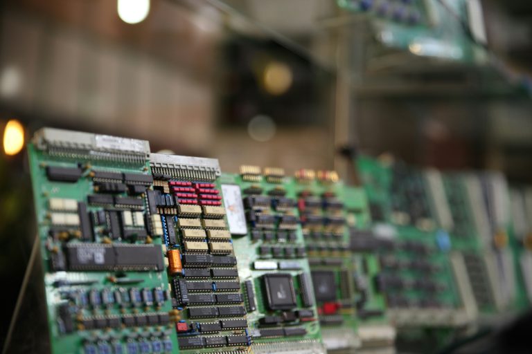
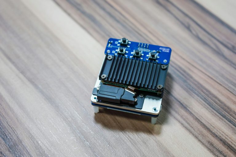
This ultimate HDI PCB manufacturing pillar content covers everything professional engineers, hardware designers, and international procurement buyers need to know about High Density Interconnect PCBs. We fully explain HDI definition, IPC-2226 standard compliance, mainstream stack structures including 1+N+1, 2+N+2, 3+N+3 and Any-Layer, microvia technical parameters, laser drilling types, complete sequential lamination workflow, industry DFM design rules, HDI vs conventional PCB comparison, practical application scenarios, common design mistakes, and professional selection guidelines. The PCB Manufacturing & Testing Guidelines, which covers all manufacturing processes from prototype to mass production, complements this HDI-focused guide. This publication follows Google E-E-A-T standards, integrates real manufacturing data and IPC official specifications, and helps you select the right HDI structure, avoid DFM pitfalls, control cost, and ensure signal integrity and production yield. Understanding hdi pcb manufacturing is essential for modern electronics design.
Table of Contents
- 1. What Is HDI PCB? Definition, Core Features & IPC Standard
- 2. HDI PCB Main Structure Types: 1+N+1, 2+N+2, 3+N+3, Any-Layer
- 3. Microvia Technology: Key Parameters, Laser Types & IPC Specifications
- 4. Complete HDI PCB Manufacturing Process Flow
- 5. HDI PCB DFM Design Rules & Critical Layout Guidelines
- 6. HDI PCB vs Conventional Through-Hole PCB: Full Comparison
- 7. HDI PCB Applications & Structure Selection Guide by BGA Pitch
- 8. Common HDI Design Mistakes & How to Avoid Them
- 9. Key Takeaways
- 10. HDI PCB FAQ
- 11. Get Custom HDI PCB Manufacturing Quote
What Is HDI PCB? Definition, Core Features & IPC Standard
HDI stands for High Density Interconnect, an advanced printed circuit board technology designed to meet the miniaturization, high integration, and high-speed signal demands of modern electronics. Defined by the official IPC-2226 standard, an HDI PCB features micro blind/buried vias, ultra-fine trace width and spacing, and much higher pad density than traditional PCBs. Understanding hdi pcb manufacturing is essential for anyone working with high-density electronic products.
Core Characteristics of HDI PCB
- Microvia instead of large mechanical through-holes
- Ultra-fine line width and narrow trace spacing
- Higher routing density in limited board area
- Shorter signal path, lower crosstalk and impedance fluctuation
- Perfect compatibility with fine-pitch BGA, QFN, CSP and high-density chips
Key Advantages
- Smaller form factor: Reduce board size by 30%–50% for compact devices
- Superior signal integrity: Ideal for high-frequency and high-speed circuits
- Higher component density: Support ultra-fine pitch chip packaging
- Better thermal & structural reliability: Optimized lamination and via filling structure
Traditional through-hole PCBs can no longer satisfy the layout requirements of flagship mobile devices, AI computing hardware, high-end wearables, server motherboards and medical electronics. HDI PCB has become the mainstream substrate for high-end industrial and consumer electronics. For fine-pitch BGA components that often require HDI structures, the BGA Fanout Techniques guide provides detailed layout recommendations that complement hdi pcb manufacturing best practices.
HDI PCB Main Structure Types: 1+N+1, 2+N+2, 3+N+3, Any-Layer
HDI PCBs are categorized by blind via stacking layers and sequential lamination design. Each structure differs in manufacturing difficulty, cost, production yield, and applicable BGA pitch. Below is the standardized classification and full comparison for hdi pcb manufacturing.
| Structure | Structural Description | Manufacturing Difficulty | Cost Level | Suitable BGA Pitch | Typical Applications |
|---|---|---|---|---|---|
| 1+N+1 | 1-layer micro blind via on top & bottom + conventional inner through-hole | Medium | Medium | 0.65mm | Consumer electronics, industrial control |
| 2+N+2 | 2-layer stepped blind via stacking on both sides | High | High | 0.5mm | High-end wearables, tablet, mid-range smartphone |
| 3+N+3 | 3-layer multi-stack blind via structure | Very High | Very High | 0.4mm & below | Server motherboard, high-end industrial control |
| Any-Layer | Full arbitrary layer interconnection | Extreme | Extreme | Ultra-fine pitch | Flagship mobile, GPU, aerospace, AI hardware |
Structure Explanation
- 1+N+1: The most cost-effective mainstream HDI type, balanced performance and budget, largest market share.
- 2+N+2: Adopts stepped stacked microvias, requires repeated lamination and laser drilling for higher density routing.
- 3+N+3: Multi-layer stacked vias demand ultra-high alignment precision, only for extreme density scenarios.
- Any-Layer HDI: Every layer can interconnect directly via microvias; maximum routing flexibility and best high-speed performance.
Proper stack-up design is critical for HDI reliability, and the Stackup Design Guide covers layer arrangements for these structures, directly supporting successful hdi pcb manufacturing.
Microvia Technology: Key Parameters, Laser Types & IPC Specifications
Microvia is the core foundation of HDI PCB manufacturing. It refers to ultra-small blind/buried vias fabricated by laser drilling, directly determining PCB yield, electrical performance and long-term reliability. Proper hdi pcb manufacturing relies heavily on microvia quality.
| Parameter | Standard Specification |
|---|---|
| Microvia Aperture | 0.075mm – 0.15mm |
| Main Laser Type | CO₂ Laser / UV Laser |
| Dielectric Thickness | ≤ 4mil |
| Maximum Aspect Ratio | ≤ 1:1 |
| Microvia Pad Margin | Aperture + 0.2mm |
Laser Drilling Type Introduction
- CO₂ Laser: Cost-effective, stable for regular resin substrates, widely used for 1+N+1 and 2+N+2 mass production.
- UV Laser: Higher positioning precision, smaller thermal damage to substrate, perfect for ultra-fine aperture and Any-Layer HDI.
Critical Microvia Design Rules
Aspect ratio controlled within 1:1 ensures uniform copper plating inside the hole; excessive ratio will cause incomplete plating, open circuit or high impedance failure. Dielectric thickness limited under 4mil guarantees reliable desmear and metallization quality for successful hdi pcb manufacturing.
Complete HDI PCB Manufacturing Process Flow
Unlike conventional PCBs with simple mechanical drilling, HDI relies on sequential lamination and multiple rounds of microvia processing. The standardized production flow for hdi pcb manufacturing is fixed as below:
Laser Drilling → Desmear → Hole Metallization → Via Fill Plating → Pattern Transfer → Etching → Sequential Lamination
Step-by-Step Process Explanation
- Laser Drilling: Drill ultra-small microvias on outer and inner layers with CO₂ or UV laser; no mechanical stress and ultra-high positioning accuracy.
- Desmear: Remove resin residue and carbonized debris on hole walls via chemical or plasma cleaning to ensure copper adhesion.
- Hole Metallization: Deposit a thin chemical copper layer on microvia walls to form conductive foundation.
- Via Fill Plating: Fully fill microvias with copper to achieve flat surface, avoid air gaps and improve high-speed signal performance.
- Pattern Transfer: Transfer circuit and pad layout via exposure and development with dry film or photosensitive ink.
- Etching: Remove redundant copper foil to form fine traces and precise pads matching HDI narrow line rules.
- Sequential Lamination: Press multi-layer substrates under high temperature and pressure; repeat lamination and drilling for 2+N+2 / 3+N+3 structures.
Manufacturing feasibility for HDI designs can be validated using the DFM Rules for High-Speed PCB, which covers line width, spacing, and via design rules essential for hdi pcb manufacturing success.
HDI PCB DFM Design Rules & Critical Layout Guidelines
To avoid production rework, low yield and high cost in hdi pcb manufacturing, designers must follow dedicated HDI DFM rules different from conventional PCBs.
Recommended Line Width & Spacing
- 1+N+1 HDI: 3/3 mil minimum line width / spacing
- Any-Layer HDI: 2/2 mil ultra-fine line capability
Microvia Pad Design
Pad diameter must be microvia aperture + 0.2mm, reserving enough tolerance for lamination alignment and laser drilling deviation.
Stacked Via Layout Rule
Adopt staggered layout or filled via alignment; direct vertical stacking will cause substrate stress, delamination and board warpage during lamination.
Additional DFM Notes
- Avoid via-in-pad over-design without factory process confirmation
- Control impedance strictly for high-speed HDI application
- Reserve enough routing space for fine-pitch BGA fanout
Accurate impedance control, which is essential for HDI signal integrity, is explained in the Impedance Matching Ultimate Guide, a key resource for hdi pcb manufacturing quality.
HDI PCB vs Conventional Through-Hole PCB: Full Comparison
| Comparison Item | HDI PCB | Conventional Through-Hole PCB |
|---|---|---|
| Routing Density | Ultra High | Low |
| Signal Integrity | Excellent for high-speed / high-frequency | Average, obvious crosstalk & loss |
| Manufacturing Process | Laser drilling + sequential lamination + via filling | Simple mechanical drilling & single lamination |
| Production Cost | Medium to Very High | Low |
| Production Cycle | Longer due to multiple processes | Short |
| Applicable Chips | 0.4mm–0.65mm fine-pitch BGA, AI, CSP | Regular SMD and through-hole components |
| Reliability & Stability | High thermal stability and anti-interference | General industrial standard |
Conventional PCBs are cost-effective for low-density simple products; HDI is the only choice for miniaturization, high-speed signal and high-density chip scenarios.
HDI PCB Applications & Structure Selection Guide by BGA Pitch
Main Application Industries
- Consumer Electronics: Smartphones, wearables, TWS earbuds
- Communication & Network: 5G module, router, baseboard
- AI & Computing: GPU, AI accelerator, server motherboard
- Medical Electronics: High-precision diagnostic equipment
- Automotive Electronics: Onboard high-speed control module
- Aerospace: High-reliability lightweight interconnect board
Quick Selection Guide for hdi pcb manufacturing
- BGA 0.65mm → Choose 1+N+1 (best cost-performance)
- BGA 0.5mm → Choose 2+N+2
- BGA 0.4mm & below → Choose 3+N+3 or Any-Layer
- Flagship high-speed AI / mobile products → Directly select Any-Layer HDI
Common HDI Design Mistakes & How to Avoid Them
| Mistake | Consequence | Correct Practice |
|---|---|---|
| Vertical stacked microvias | Delamination and warpage | Use staggered layout |
| Exceed 1:1 microvia aspect ratio | Plating failure | Strictly control dielectric thickness |
| Too small microvia pad | Misalignment, open circuit | Reserve 0.2mm margin as standard |
| Overly fine lines without checking capability | Low yield, rework | Follow 3/3 mil and 2/2 mil standard rules |
| Ignore IPC-2226 compliance | Certification failure | Always design according to official HDI standard |
Avoiding these mistakes can greatly improve production yield and save redesign cost and lead time in hdi pcb manufacturing.
Key Takeaways
- HDI PCB is defined by IPC-2226, relying on microvia, fine trace and sequential lamination to achieve high-density interconnection
- 1+N+1, 2+N+2, 3+N+3 and Any-Layer cover all density demands; 1+N+1 is the mainstream cost-effective option for hdi pcb manufacturing
- Microvia parameters, laser drilling type and aspect ratio are the core of HDI manufacturing quality
- The complete HDI workflow follows fixed sequential lamination steps, far more complex than traditional PCB
- Following HDI DFM rules can avoid DFM errors, low yield and extra cost
- Select HDI structure according to BGA pitch, product positioning and budget to achieve optimal balance of cost, performance and reliability
HDI PCB FAQ
Q1: What does 1+N+1 mean in HDI PCB?
1 layer of micro blind via on top and bottom outer layers, with N inner conventional layers and through-hole interconnection; the most popular entry-level HDI structure in hdi pcb manufacturing.
Q2: What is the smallest microvia size for HDI manufacturing?
Standard mass production aperture ranges from 0.075mm to 0.15mm, controlled under IPC-2226 specification.
Q3: What is the difference between CO₂ laser and UV laser for microvia drilling?
CO₂ laser is cost-effective for regular HDI; UV laser has higher precision for ultra-fine aperture and Any-Layer PCB.
Q4: Is Any-Layer HDI much more expensive than 1+N+1?
Yes, Any-Layer has extremely high process difficulty and material cost, only recommended for flagship high-end products.
Q5: Can I use 3/3 mil line width for 1+N+1 HDI?
Yes, 3/3 mil is the safe standard for mass production; Any-Layer can support 2/2 mil ultra-fine lines.
Q6: What BGA pitch fits 1+N+1 HDI?
Perfect for 0.65mm pitch BGA, covering most consumer and industrial control products.
Get Custom HDI PCB Manufacturing Quote
Whether you need 1+N+1, 2+N+2, 3+N+3 or Any-Layer HDI PCB design verification, prototype manufacturing, or mass production, our professional engineering team can provide one-stop service including DFM review, stackup design, parameter optimization, and customized quotation for your hdi pcb manufacturing project.
We offer: DFM review • Stackup design • Parameter optimization • Prototype manufacturing • Mass production
Send your Gerber files, specify layer count, BGA pitch and special requirements. We will reply with a fast official HDI PCB quote and technical solution within 24 hours.
About HighSpeedPCBs.com
We are a specialized PCB design and manufacturing service provider serving industrial, automotive, medical, and communications OEMs worldwide. Our expertise in hdi pcb manufacturing ensures your high-density designs are producible and cost-effective. Complete manufacturing process documentation is available in the PCB Manufacturing & Testing Guidelines.
© 2026 HighSpeedPCBs.com — Professional High-Speed PCB Solutions