In high-speed PCB design, via transitions ruin impedance control by introducing capacitance and inductance that create signal reflections. This pillar page explains the physics, real-world impacts, and proven fixes for maintaining consistent 50Ω impedance through via structures.
The Physics of How Via Transitions Ruin Impedance Control PCB
Capacitive and Inductive Nature of Vias
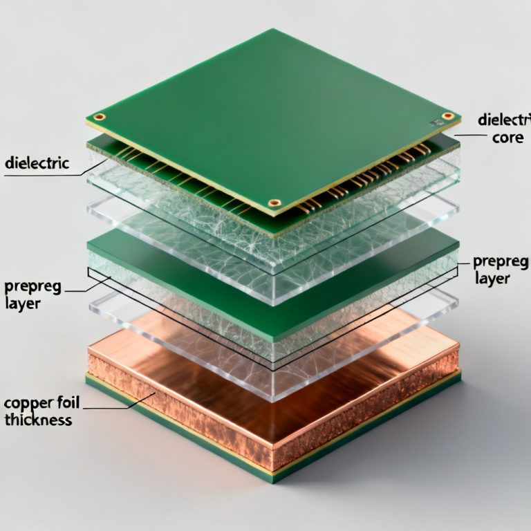
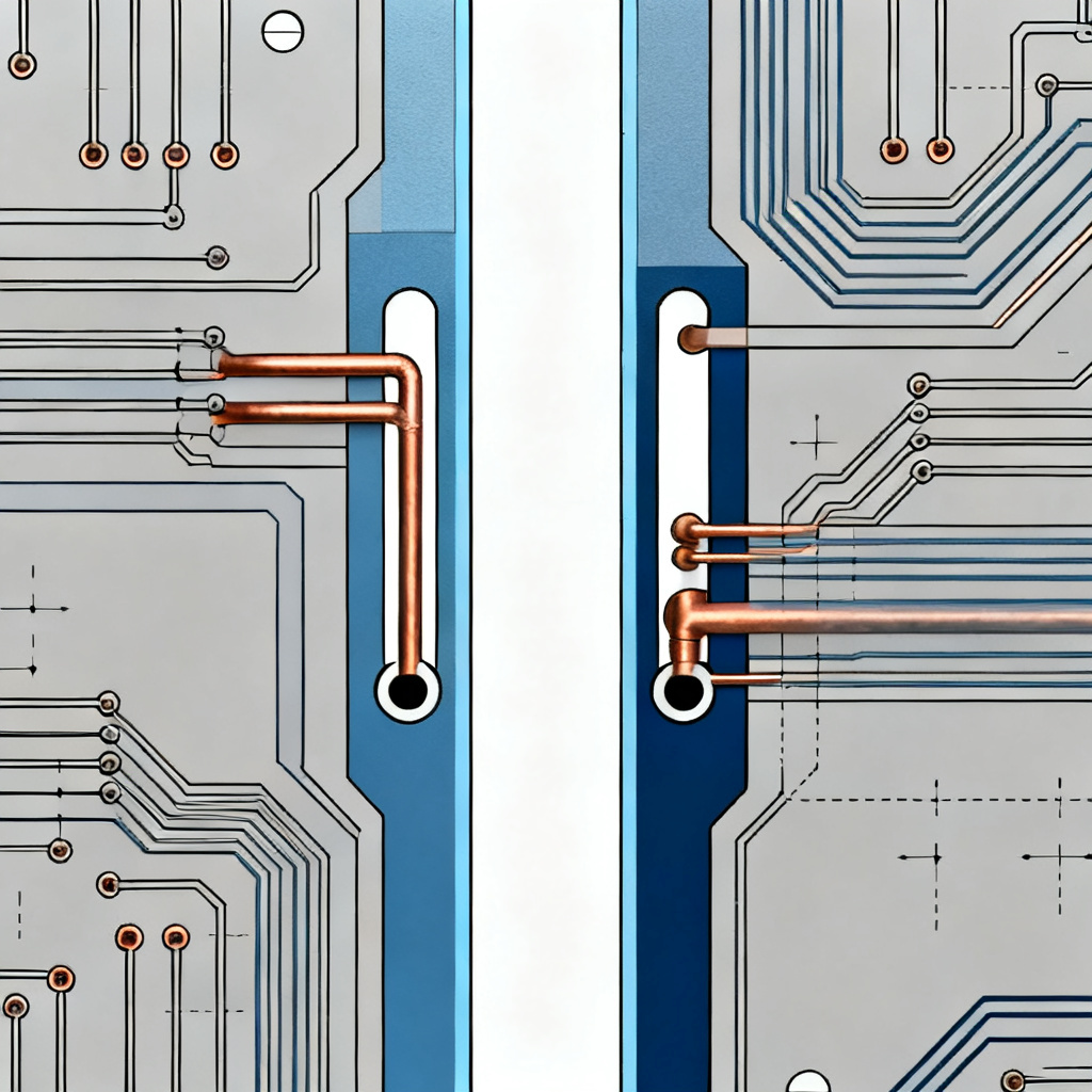
A via is not a simple conductor; it is a discrete reactive element. When a signal transitions from a microstrip on the top layer to a stripline on an inner layer, the via barrel, pad, and anti-pad create excess capacitance (C) and excess inductance (L). The net effect is a low-impedance dip due to capacitance followed by a high-impedance peak due to inductance, creating a resonant discontinuity that ruins impedance control.
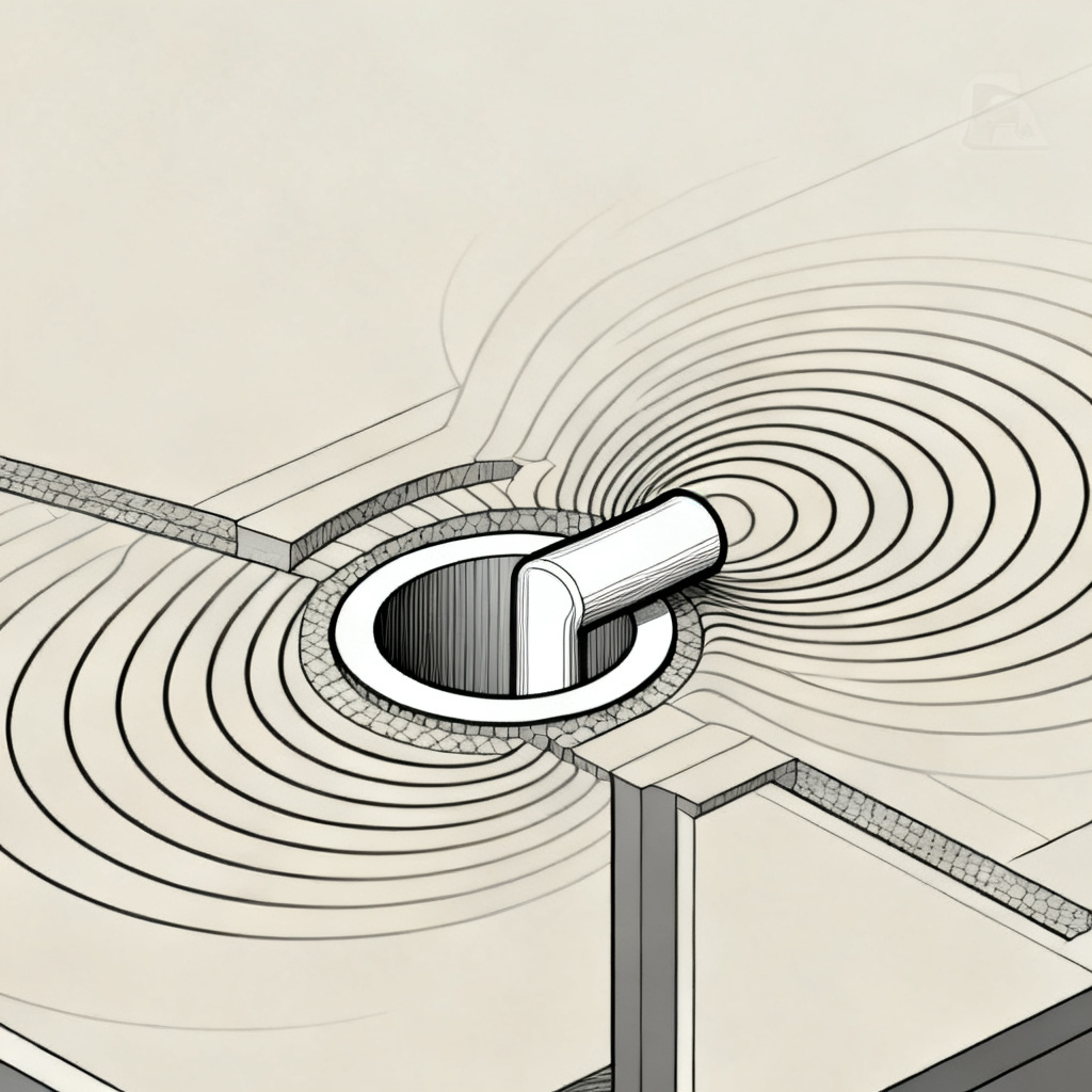
Stub Resonance: The Stub Antenna Effect
The most destructive via artifact is the stub—the unused portion of the via barrel extending beyond the signal layer to the bottom of the board. A stub acts as a quarter-wave transmission line at certain frequencies. When the stub length equals λ/4 of the signal’s harmonic, it creates a short circuit at the via junction, causing notch filter behavior and return loss spikes. The stub length should be kept below 1/10th of the signal’s wavelength to avoid significant degradation.
Real-World Impacts: How Via Transitions Ruin Impedance Control PCB
Impedance Mismatch Causes Reflection and Jitter
Every via transition introduces a discontinuity. The reflection coefficient (Γ) is proportional to the impedance mismatch. A 50Ω trace sees a via with 35Ω effective impedance, causing 18% of signal energy reflected. This reflected energy travels back to the driver, causing overshoot, undershoot, and ringing. In high-speed digital (e.g., PCIe Gen4, 25 Gbps), even 5% reflected energy can cause eye closure and timing jitter.
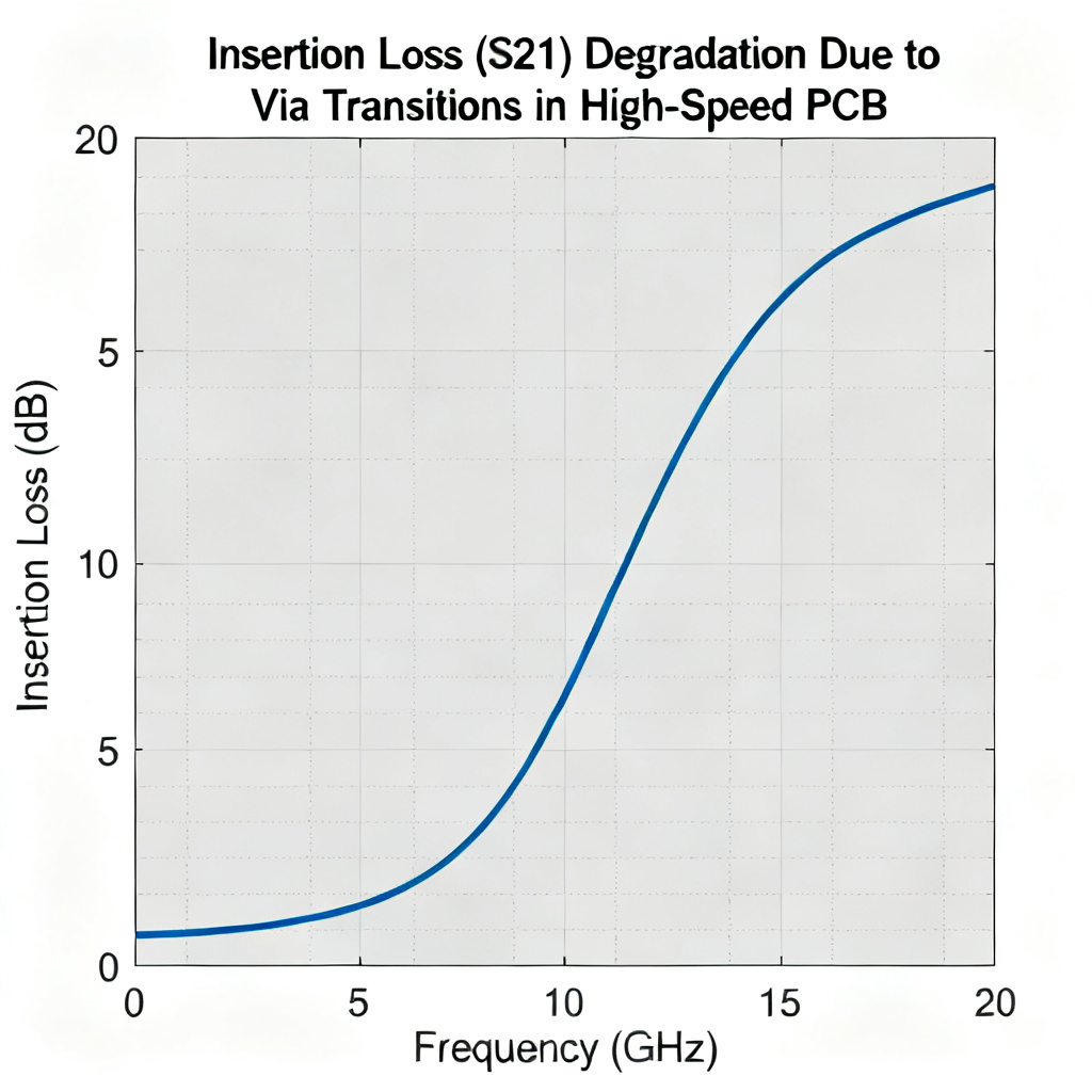
Insertion Loss (S21) Degradation
Measured data shows a single via with a 30-mil stub at 10 GHz can add 0.5–1.0 dB of insertion loss. A back-drilled via (stub removed) reduces loss to less than 0.1 dB at the same frequency. Multiple via transitions compound the loss, making the channel non-compliant with standards like 10GBASE-KR.
Mode Conversion and Radiation
Unbalanced via structures cause common-mode noise and electromagnetic radiation. The via acts as a slot antenna if the return current path is broken, causing crosstalk to adjacent traces and radiated EMI failures.
Manufacturing Tolerance Sensitivity
Even with perfect design, fabrication tolerances can ruin impedance. Pad size variation of ±2 mils can shift impedance by ±2–3Ω. Anti-pad etching and dielectric thickness variation also contribute to impedance deviation.
How to Fix Via Transitions That Ruin Impedance Control PCB
Back-Drilling (Controlled Depth Drilling)
Back-drilling removes the unused via stub from the bottom of the board. The back-drill bit diameter is slightly larger than the original via drill size (typically +8–12 mils). Use back-drilling for signals > 1 GHz or when the stub length exceeds 1/10th of the signal wavelength. Specify a maximum stub remnant of 5–10 mils in your fabrication notes. Back-drilling adds 15–30% to PCB cost but is mandatory for 10+ Gbps signals.
Optimize Via Pad and Anti-Pad Geometry
Reduce via pad diameter to minimize parasitic capacitance. For a 50Ω via, use the smallest pad allowed by your fabricator’s capability (e.g., 18-mil pad for a 10-mil drill). Increase anti-pad clearance to reduce capacitance but not so large that it creates an inductive loop. For differential vias, use oval or rectangular anti-pads to match the pair’s geometry and reduce common-mode conversion.
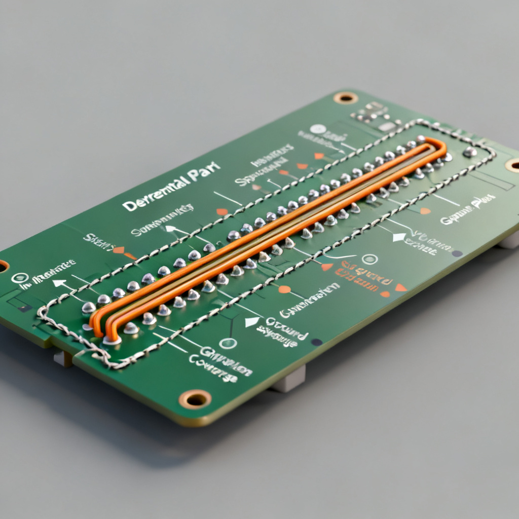
Add Ground Via Stitching
Vias carrying high-speed signals require a return current path directly adjacent to them. Place a ground via within 1.5× the dielectric thickness (e.g., within 10–15 mils for a 10-mil dielectric) of each signal via. For differential pairs, place ground vias symmetrically around the pair. For critical channels, create a “fence” of ground vias on both sides of the signal via array, spaced at λ/20 or less.
Use Microvias and Buried Vias
Microvias (laser-drilled) have much smaller capacitance than mechanical vias because they are shorter (typically 3–5 mils), have smaller pad diameters (12–14 mils), and eliminate stubs entirely when used as blind vias. Buried vias connect only inner layers and do not extend to the surface, eliminating the stub issue for those layers. These solutions increase cost but are best for ultra-high-density designs (e.g., 50+ Gbps).
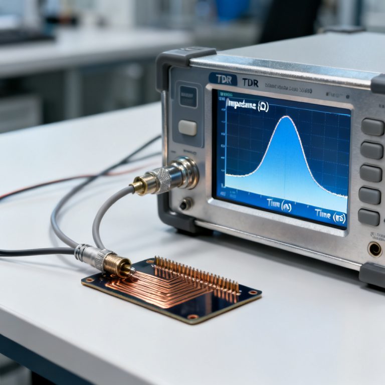
Simulate and Tune the Via Structure
Use full-wave 3D EM solvers (e.g., Ansys HFSS, CST, or Keysight ADS) to model the via’s S-parameters up to the 5th harmonic of your signal. Adjust pad size, anti-pad size, and ground via placement iteratively. Target keeping the via’s impedance within 10% of the target impedance (e.g., 45–55Ω for a 50Ω system).
For Differential Pairs: Symmetry is Everything
Differential vias must be perfectly symmetric to maintain odd-mode impedance and suppress common-mode noise. Use identical via geometry for both P and N signals. Ensure the ground vias are equidistant from both signal vias. Avoid routing differential traces into vias at 90° angles; use a 45° entry to reduce impedance mismatch.
Step-by-Step Design Workflow for Impedance Control PCB Via Fixes
- Define your signal speed and bandwidth: Calculate the maximum frequency (e.g., 0.35/rise_time). For a 25 ps rise time, the knee frequency ≈ 14 GHz.
- Determine stub length tolerance: If the stub length > 1/10th wavelength at the knee frequency, specify back-drilling.
- Select via geometry: Drill size as small as your fabricator can reliably plate (e.g., 8–10 mils for standard; 4–6 mils for HDI). Pad size = drill size + 10 mils minimum. Anti-pad size = pad size + 2× dielectric thickness.
- Add ground vias: One ground via per signal via, placed within 15 mils.
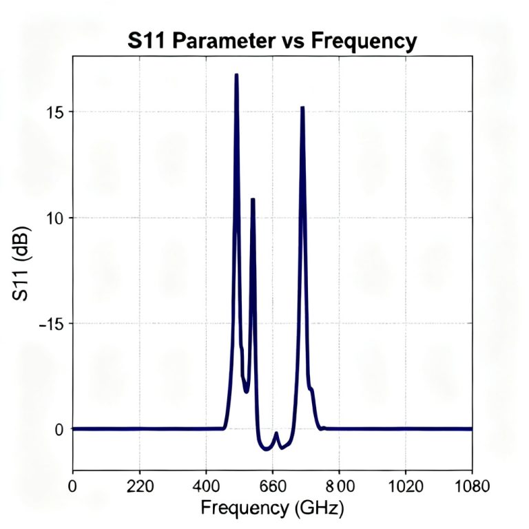
- Simulate: Run a 3D EM simulation of a single via transition. Check S11 < -20 dB and S21 > -0.5 dB at your operating frequency.
- Review fabrication capabilities: Ensure your fabricator can achieve the specified back-drill depth tolerance (±5 mils) and anti-pad etching tolerance (±2 mils).
- Document in your stack-up: Include via impedance targets in your PCB fabrication drawing.
Comparison: Via Fix Methods for Impedance Control PCB
| Fix Method | Impedance Control PCB Benefit | Cost Impact | Best For |
|---|---|---|---|
| Back-Drilling | Eliminates stub resonance, reduces insertion loss by 0.5–1.0 dB | +15–30% | 1–10 GHz signals |
| Optimized Pad/Anti-Pad | Reduces parasitic capacitance, maintains 50Ω target | Minimal | All high-speed designs |
| Ground Via Stitching | Provides return current path, reduces inductance | Minimal | Differential pairs, RF channels |
| Microvias/Buried Vias | Eliminates stubs, reduces capacitance by 50% | +30–50% | 50+ Gbps, HDI designs |
| Full-Wave Simulation | Validates impedance within 5% tolerance | Engineering time | All critical channels |
Common Mistakes That Ruin Impedance Control PCB and How to Avoid Them
| Mistake | Consequence | Fix |
|---|---|---|
| Using large via pads (e.g., 30 mils for a 10-mil drill) | Low impedance dip (35–40Ω) | Reduce pad to 20–22 mils |
| No ground vias near signal vias | High inductance, mode conversion | Add ground vias within 15 mils |
| Ignoring stub length for 5+ GHz signals | Resonant loss at frequency harmonics | Back-drill or use blind vias |
| Asymmetric differential via pair | Common-mode noise, EMI | Mirror geometry and ground via placement |
| Using thermal relief on high-speed vias | Increased inductance, poor return path | Use full copper connection |
Key Terminology for Impedance Control PCB Via Design
Stub: The unused portion of a via barrel that extends beyond the signal layer, causing quarter-wave resonance and signal degradation.
Back-drilling: A secondary drilling operation that removes the via stub to eliminate resonance.
Anti-pad: The clearance hole in ground or power planes around a via, which controls parasitic capacitance.
Return current path: The path that signal return current takes, which must be continuous to maintain impedance.
Mode conversion: The transformation of differential-mode signals into common-mode noise due to asymmetric via structures.
Insertion loss (S21): The loss of signal power as it travels through a via transition, measured in dB.
Frequently Asked Questions About Via Transitions and Impedance Control PCB
How do via transitions ruin impedance control PCB?
Via transitions ruin impedance control PCB by introducing parasitic capacitance and inductance, creating impedance discontinuities that cause signal reflections, insertion loss, and jitter. The via stub acts as a quarter-wave resonator at certain frequencies, further degrading signal integrity.
What is the best method to fix via transitions for impedance control PCB?
Back-drilling is the most effective method to fix via transitions for impedance control PCB, as it removes the resonant stub. Combining back-drilling with optimized pad/anti-pad geometry and ground via stitching provides the best impedance control for high-speed signals.
How does stub length affect impedance control PCB performance?
Stub length directly affects impedance control PCB performance by creating a resonant notch in the insertion loss. When the stub length equals λ/4 of the signal frequency, it causes a short circuit at the via junction. Keeping stub length below 1/10th of the signal wavelength prevents significant degradation.
Can microvias improve impedance control PCB?
Yes, microvias significantly improve impedance control PCB because they are shorter (3–5 mils), have smaller pad diameters, and eliminate stubs when used as blind vias. This reduces parasitic capacitance and inductance, maintaining consistent impedance for ultra-high-speed designs.
What is the role of ground vias in impedance control PCB?
Ground vias provide a low-inductance return current path for signal vias, which is critical for maintaining impedance control PCB performance. Without ground vias, the return current must find a longer path, increasing inductance and causing impedance mismatch and common-mode noise.
“`