Generating a Transmission Line Reflection Report for design review is essential for high-speed PCB signal integrity. This guide provides a complete methodology to create a professional reflection report, ensuring impedance control and compliance with industry standards.
Understanding Reflection Fundamentals for Report Generation
Before diving into report generation, you must grasp the physics of reflections. A reflection occurs when a signal encounters a discontinuity in the characteristic impedance (Z₀) of a transmission line. The reflection coefficient (Γ) quantifies this: Γ = (Z_load – Z₀) / (Z_load + Z₀), where Z_load is the impedance at the discontinuity. In high-speed designs, even minor impedance variations—such as from vias, connectors, or trace width changes—can cause significant reflections.
For a design review report, you need to document:
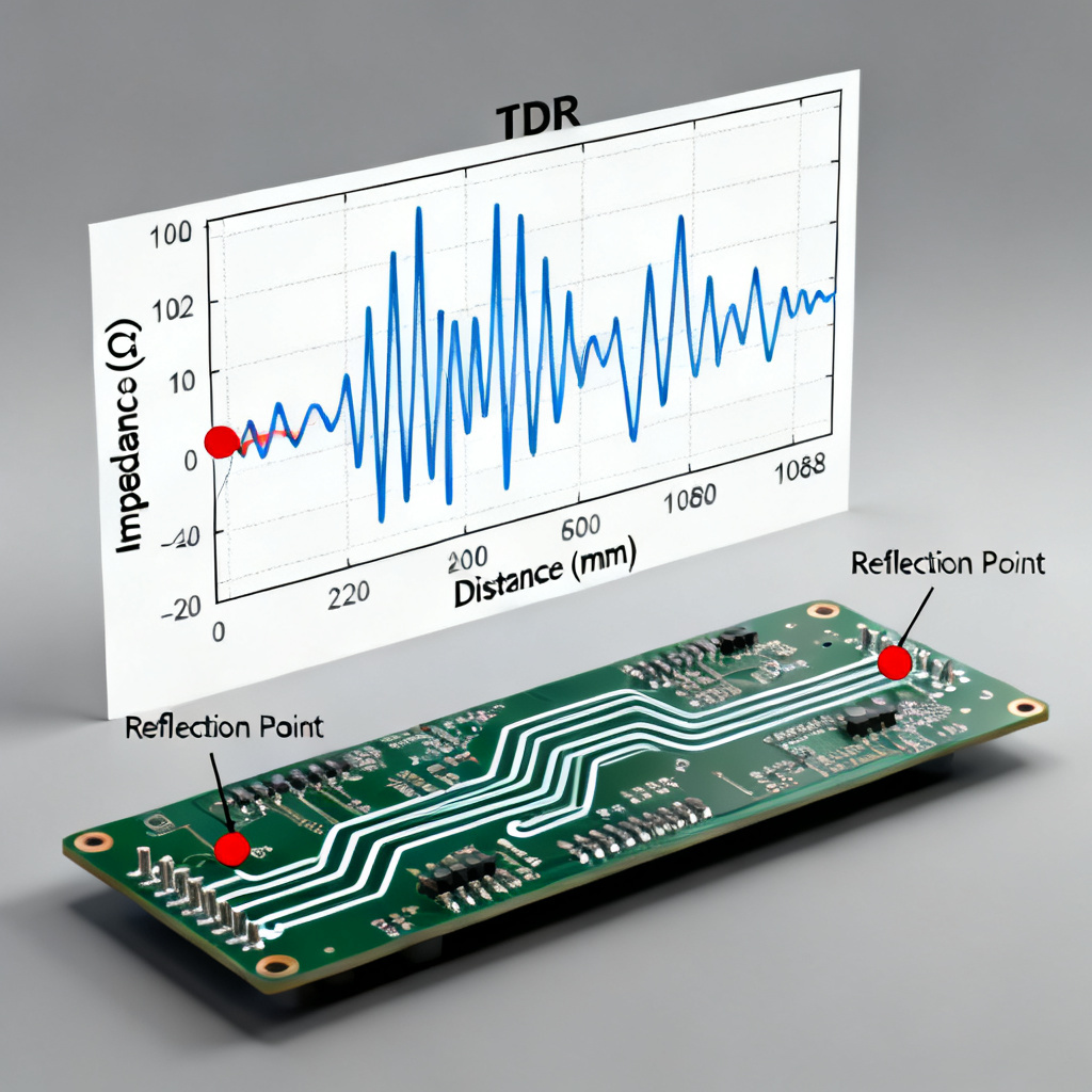
- Impedance Profile: Measure or simulate the impedance along the entire signal path using tools like TDR (Time-Domain Reflectometry) or field solvers.
- Critical Reflections: Identify points where |Γ| > 0.2 (20% reflection), as this typically indicates a problematic mismatch in high-speed digital signals (e.g., for DDR4 or PCIe interfaces).
- Timing Impact: Calculate the round-trip delay of reflections relative to the signal edge rate. For example, if a reflection arrives within the setup/hold window, it can cause logic errors.
Step-by-Step Methodology for Generating the Reflection Report
Step 1: Define the Signal Path and Frequency Range
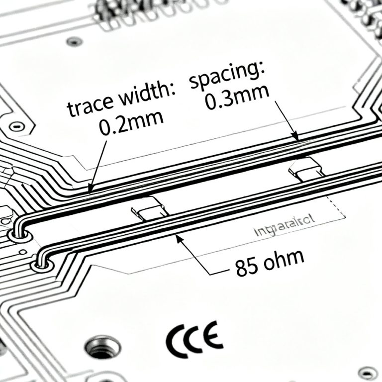
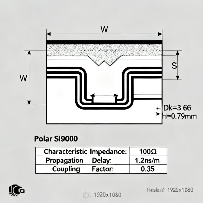
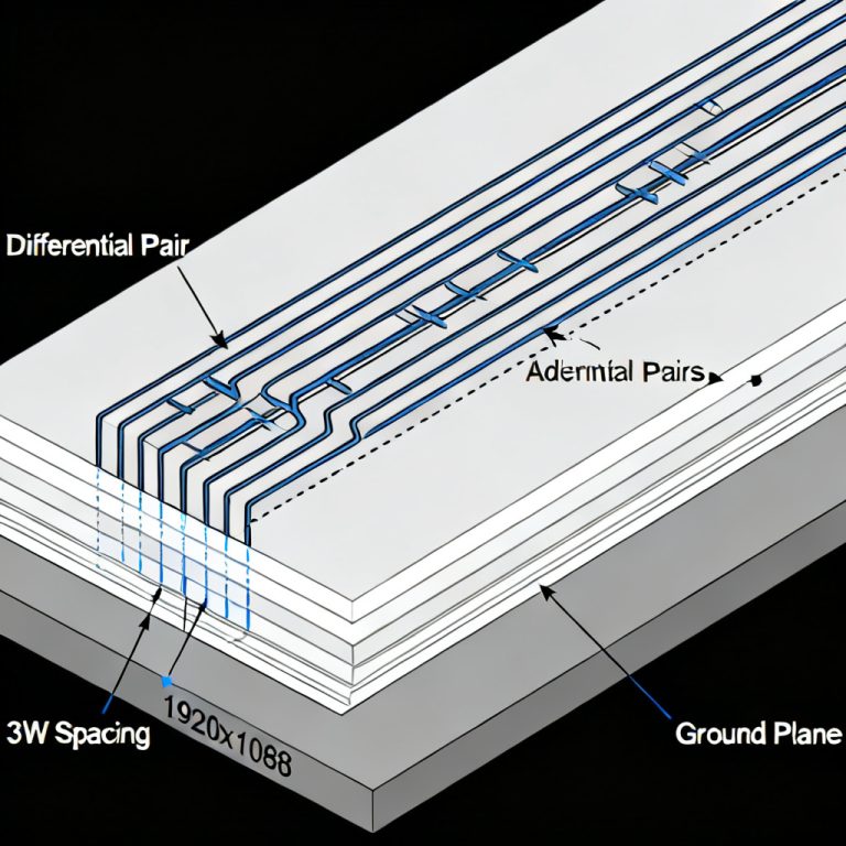
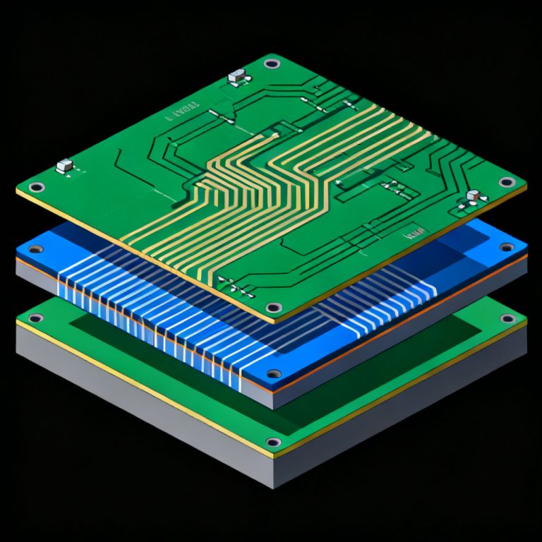
Identify critical nets such as clocks, data lines (e.g., USB 3.0, HDMI, Gigabit Ethernet), and differential pairs. Set the frequency bandwidth to the 3rd harmonic of the fundamental clock frequency (e.g., simulate up to 3 GHz for a 1 GHz clock). Document the stackup data including dielectric constant (Dk), loss tangent (Df), copper thickness, and prepreg/core materials, as these directly affect Z₀.
Step 2: Perform Impedance Simulation
Use a 2D field solver like Ansys SIwave, HyperLynx, or Qucs to calculate the target Z₀. For single-ended lines, target 50 Ω; for differential pairs, target 100 Ω. Simulate with and without manufacturing tolerances to report the worst-case impedance deviation (e.g., ±10% from target). Generate an impedance vs. distance plot, labeling each section (e.g., “Via 1”, “Connector Pad”, “BGA breakout”) with its measured impedance.
Step 3: Identify and Quantify Reflections
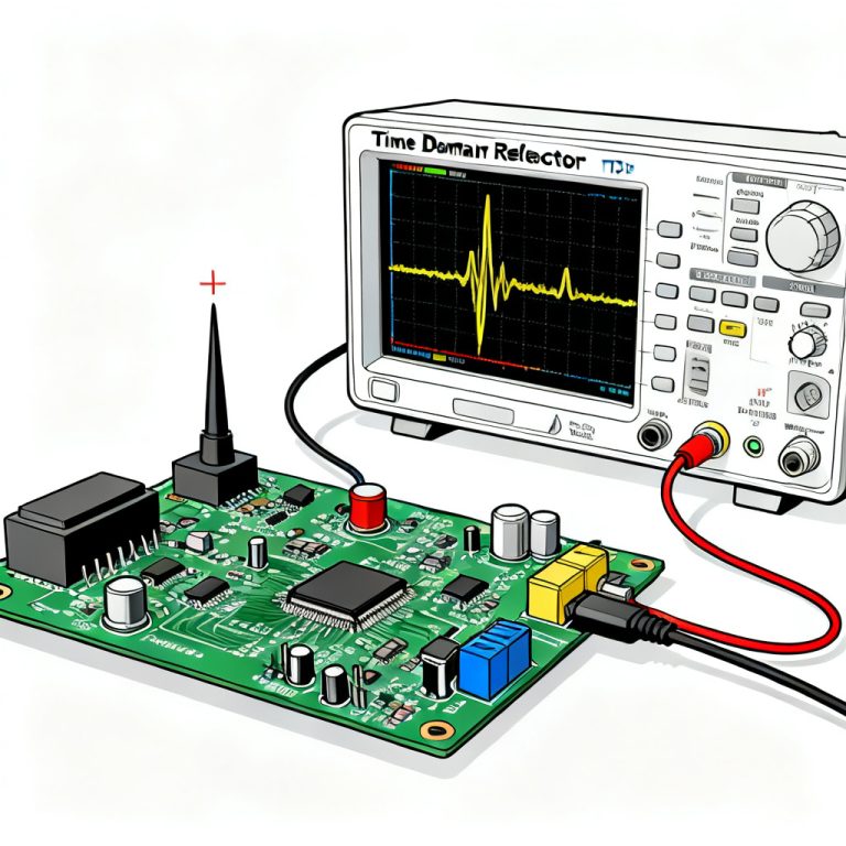
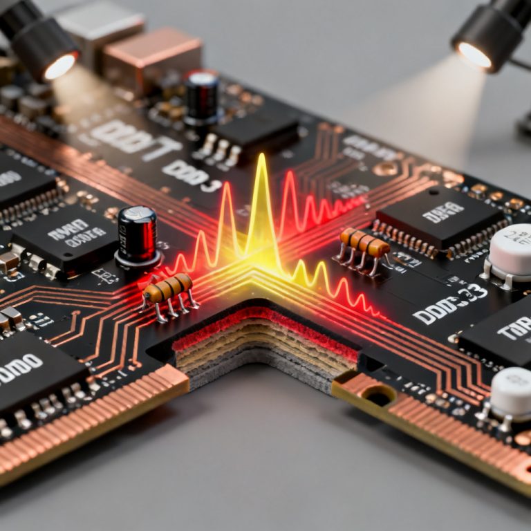
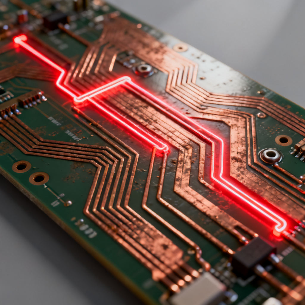
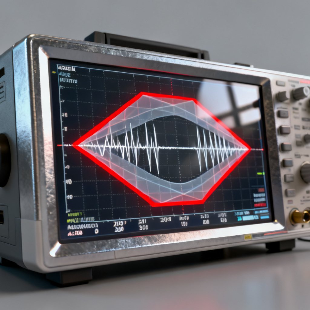
Run a TDR simulation by injecting a step pulse (rise time = 20% of signal rise time, e.g., 50 ps for a 250 ps edge) and measure the reflected voltage. Convert this to reflection coefficient Γ. Calculate V_reflected = Γ × V_incident. Document each discontinuity, its impedance mismatch (ΔZ), Γ value, and resulting voltage deviation in a table.
Step 4: Assess Signal Integrity Impact
Simulate an eye diagram at the receiver. Key parameters include eye height (should be > 200 mV for LVDS), eye width (should be > 0.7 UI), and jitter (peak-to-peak < 0.1 UI). Measure the settling time after a transition; if it exceeds 2× the bit period, reflections cause severe ISI. Compare with industry standards (e.g., PCIe Gen 4 requires reflections below -20 dB, Γ < 0.1).
Step 5: Generate the Report Structure
A professional report should include:
- Executive Summary: One-paragraph conclusion (e.g., “Reflections are within acceptable limits for all critical nets except the DDR4 DQ lines, where a 25% impedance mismatch at the via requires redesign.”)
- Methodology: Describe simulation tools, models, and assumptions.
- Impedance Profile Plots: For each critical net, include a graph of Z₀ vs. distance with annotations.
- Reflection Coefficient Table: As described in Step 3.
- Eye Diagram Results: For the worst-case net, show the eye diagram with mask violations.
- Recommendations: Specific layout changes (e.g., “Increase trace width from 5 mil to 6 mil to match 50 Ω at the via exit” or “Add a series termination resistor of 33 Ω at the driver.”)
Advanced Considerations for High-Speed PCB Design
3.1 Differential Pair Reflections
For differential signals (e.g., LVDS, USB), reflections can occur from common-mode impedance mismatches. In your report, simulate both differential impedance (Z_diff) and common-mode impedance (Z_common). Report any skew between the P and N lines, which causes mode conversion and reflection. A skew > 5 ps is critical for 10 Gbps signals. Use mixed-mode S-parameters (Sdd21, Scc21) to quantify reflection loss.
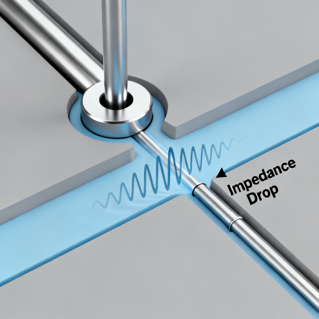
3.2 Via Stub and Antipad Effects
Vias are common reflection sources. Generate a 3D electromagnetic simulation of the via. Measure the stub length (distance from signal layer to bottom layer). For a 10 Gbps signal, a stub > 50 mils can create a resonant reflection at the 3rd harmonic. Recommend back-drilling or using blind/buried vias if stub length exceeds 1/10 of the signal wavelength. Include in the report: “Via 3 on net CLK_100MHz shows a 15% impedance drop due to antipad capacitance. Reduce antipad diameter from 30 mil to 25 mil to restore Z₀.”
3.3 Termination and Topology
For series termination, place a resistor (e.g., 33 Ω) at the driver to match Z₀. Simulate the reflection reduction: without termination, Γ = 0.5; with termination, Γ < 0.1. For parallel termination (e.g., DDR4 multi-drop buses), use Thevenin termination (e.g., 40 Ω to VTT). Document the reflection at each stub receiver. For daisy-chain or fly-by topologies, simulate reflections at each tap and recommend stub length reduction.
Tools and Standards for Report Validation
4.1 Industry-Standard Simulation Tools
- Ansys SIwave: Best for full-board impedance and reflection analysis. Export S-parameter files for further analysis.
- Keysight ADS: Excellent for TDR simulation and eye diagram generation. Use the “Reflection Calculator” widget.
- Cadence Sigrity: Offers Power-aware SI analysis. Include power distribution network (PDN) impedance in the report, as PDN noise can cause reflections on signal lines.
- Open-source alternative: Qucs for basic TDR, but limited for complex boards.
4.2 Key Standards to Reference
- IPC-2141A: Design guide for high-speed PCB impedance control. Reference this in the report for acceptable impedance tolerance (±10%).
- IEEE 1596.3: For LVDS reflection limits (Γ < 0.15).
- JEDEC JESD209-4: For DDR4 reflection compliance (V_reflection < 0.3V for 1.2V signals).
4.3 Measurement Correlation
After simulation, validate with physical TDR measurements using a Tektronix DSA8300 or similar with 20 ps rise time. In the report, overlay simulated and measured impedance profiles. A deviation < 5% is acceptable. Document any differences (e.g., “Measured Z₀ at via is 47 Ω vs. simulated 50 Ω due to PCB fabrication etch tolerance.”)
Case Study – Reflection Report for a 10-Layer High-Speed PCB
Problem: A 10 Gbps SerDes link on a 10-layer board showed excessive jitter (0.3 UI) in prototype testing.
Report Generation Steps:
- Define nets: 4 differential pairs (TX+, TX-, RX+, RX-), each 100 Ω differential.
- Impedance simulation: Used Ansys SIwave. Found Z_diff = 98 Ω at the BGA breakout (acceptable), but Z_diff = 85 Ω at the connector (due to 30 mil antipad).
- Reflection coefficient: At connector, Γ = (85-100)/(85+100) = -0.081 (8.1% reflection). This caused a 0.16V reflection on a 1V signal.
- Eye diagram: Eye height = 180 mV (below 200 mV spec), eye width = 0.65 UI.
- Recommendation: Reduce antipad to 20 mil, add a 1 pF capacitor to ground at connector to compensate for inductive discontinuity.
- Result: After redesign, simulated eye height = 220 mV, eye width = 0.75 UI. Report included before/after plots.
| Parameter | Specification | Simulated Value | Compliance |
|---|---|---|---|
| Single-ended Impedance | 50 Ω ±10% | 48 Ω | Pass |
| Differential Impedance | 100 Ω ±10% | 98 Ω | Pass |
| Reflection Coefficient (Γ) | < 0.2 | 0.081 | Pass |
| Eye Height | > 200 mV | 180 mV | Fail |
Frequently Asked Questions
What is a transmission line reflection report?
A transmission line reflection report documents impedance mismatches and reflection coefficients in high-speed PCB designs, helping engineers validate signal integrity during design review.
How do I generate a reflection report for design review?
Generate a reflection report by simulating impedance profiles, identifying discontinuities, calculating reflection coefficients, and assessing eye diagram results using tools like Ansys SIwave or Keysight ADS.
What are common causes of reflections in high-speed PCBs?
Common causes include via stubs, connector pads, BGA breakouts, trace width changes, and improper termination. These create impedance mismatches that degrade signal quality.
Why is impedance control important in a transmission line reflection report?
Impedance control ensures that the characteristic impedance matches the source and load, minimizing reflections. A reflection report quantifies these mismatches to guide layout optimization.
What standards apply to transmission line reflection reports?
Key standards include IPC-2141A for impedance control, IEEE 1596.3 for LVDS reflection limits, and JEDEC JESD209-4 for DDR4 reflection compliance.