In high-speed PCB design, Reflection in Transmission Line at T-Junctions and Branch Points is a critical signal integrity challenge. This guide covers physics, modeling, and mitigation for custom high-speed PCB manufacturing.
Physics of Reflection in Transmission Line at T-Junctions and Branch Points
What is a T-Junction in a Transmission Line?
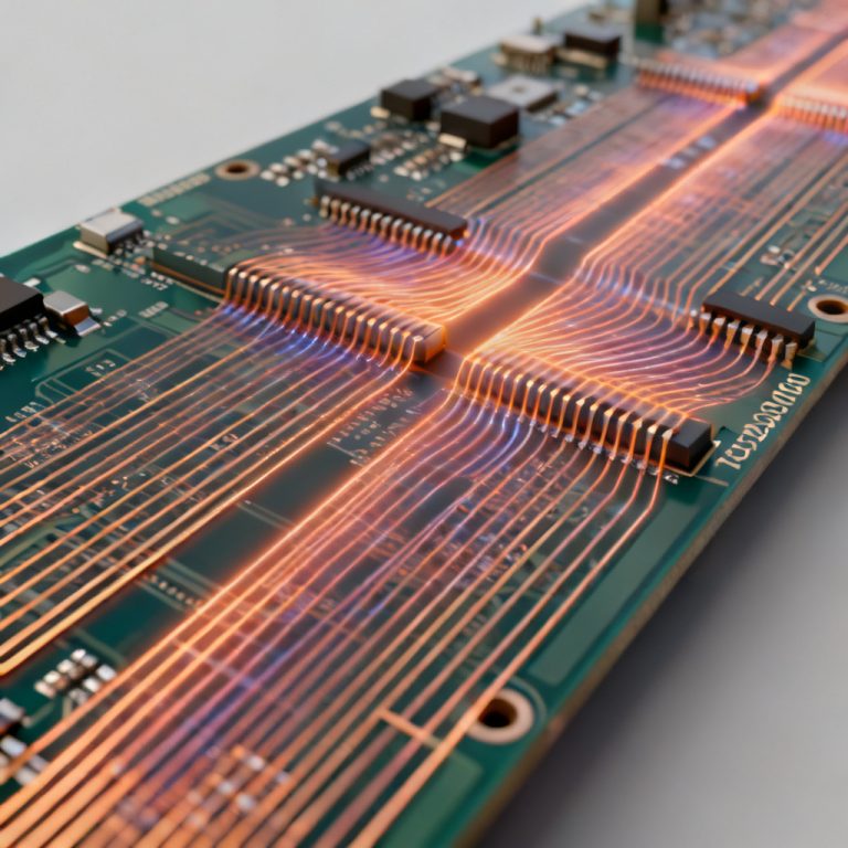
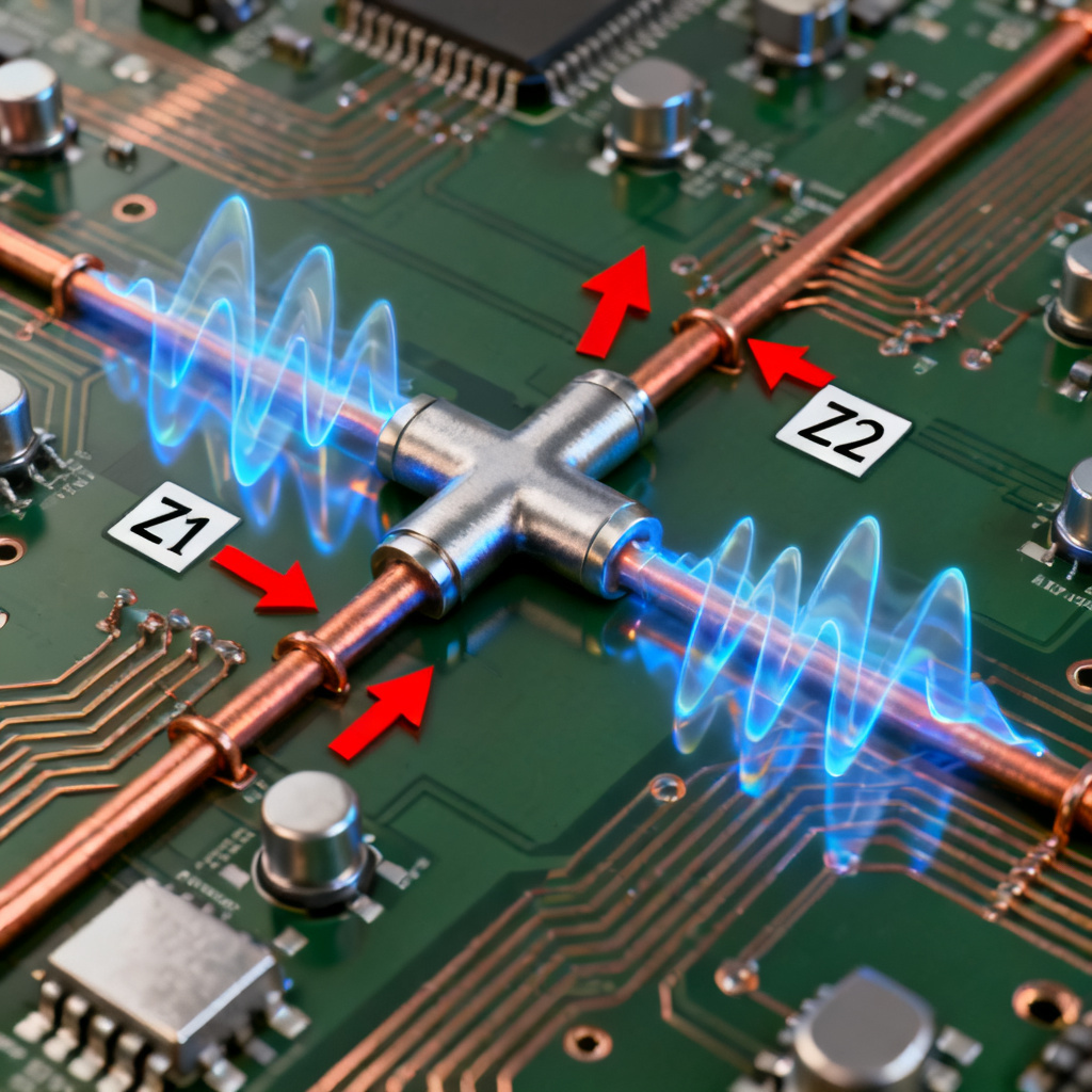
A T-junction (or branch point) is a discontinuity where a main transmission line splits into two or more branches. In high-speed PCB design, this occurs when a clock signal fans out to multiple loads, creating an abrupt change in characteristic impedance (Z0).
Why Does Reflection Occur?
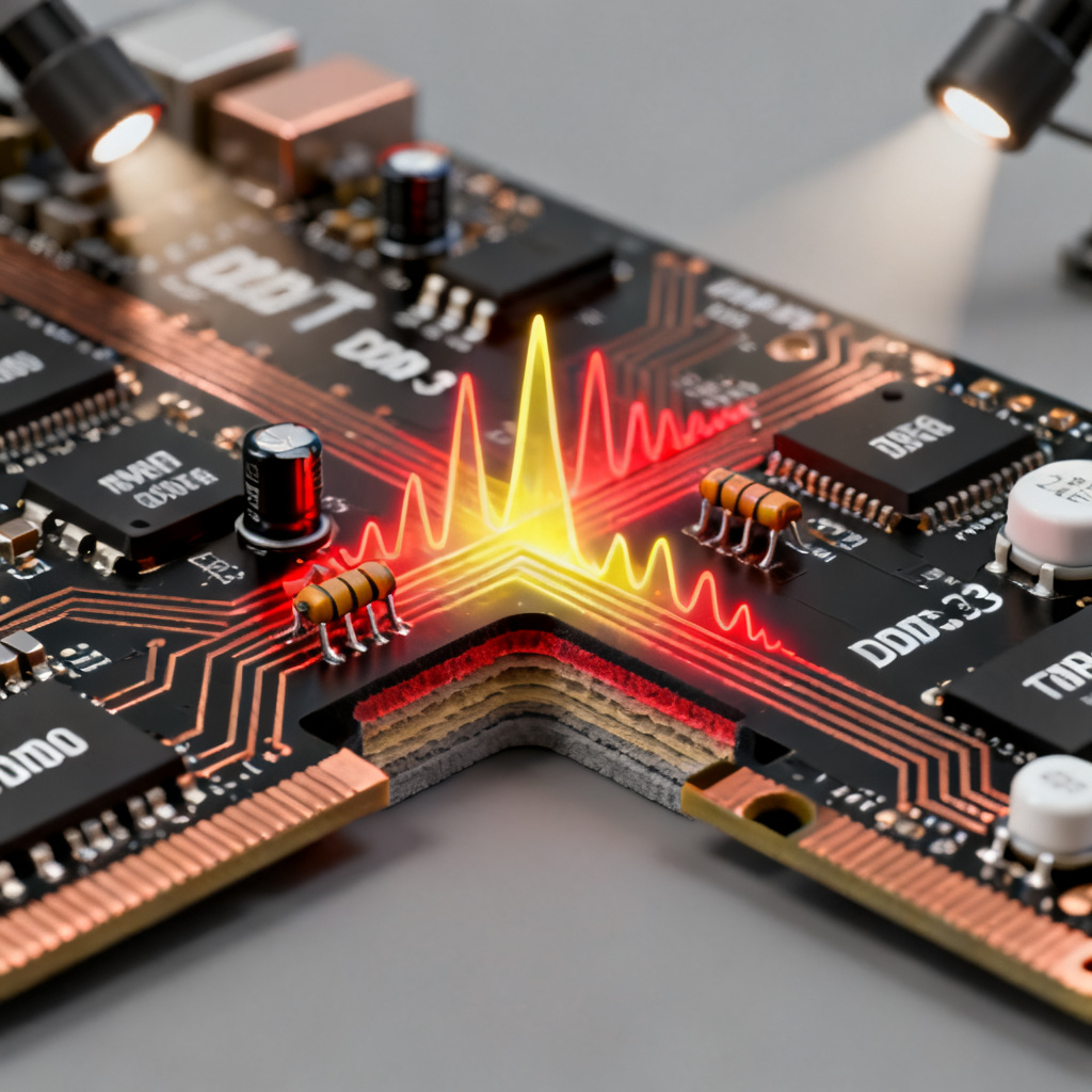
Reflection happens because the T-junction presents an impedance discontinuity. The incident signal sees a sudden change in Z0, and a portion of the signal energy is reflected. The reflection coefficient (Γ) is:
Γ = (Z_load – Z0) / (Z_load + Z0)
For two identical branches (each Z0 = 50Ω), Z_load = 25Ω, giving Γ = -0.333, meaning 33.3% of the signal is reflected with opposite polarity.
Types of Reflections at Branch Points
Impedance Mismatch Reflection: The parallel combination of branches lowers effective impedance, causing negative reflection.
Stub Resonance Reflection: A branch line λ/4 long acts as an open circuit, reflecting the entire signal.
Time-Domain Reflections: Cause ringing, overshoot, and increased rise/fall times in digital signals.
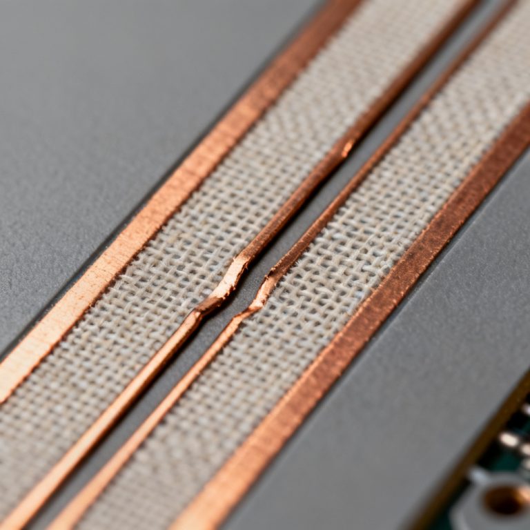
Role of Stub Length
For stubs shorter than λ/10, reflection is mainly due to impedance mismatch. Longer stubs act as transmission lines, and their termination creates additional reflections. Stubless techniques like via-in-pad are essential for high-speed PCB design.
Mathematical Modeling of Reflection in Transmission Line at T-Junctions
Reflection Coefficient for Multiple Branches
For N identical branches, Z_load = Z0 / N, so Γ = (1/N – 1) / (1/N + 1). For N=2, Γ = -0.333; for N=3, Γ = -0.5. Fan-out increases reflection proportionally.
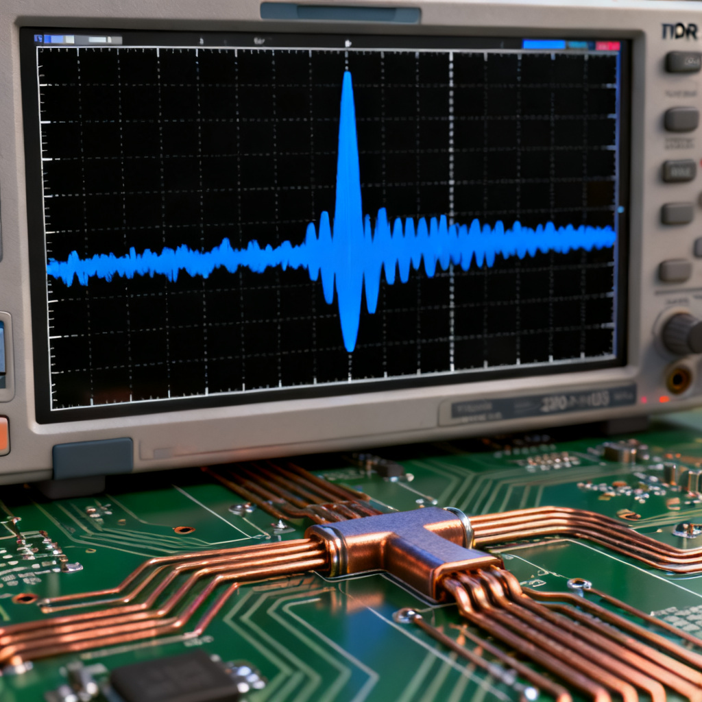
Time-Domain Reflectometry (TDR) Analysis
TDR measures reflections by launching a step pulse. At a T-junction, the TDR trace shows a dip from 50Ω to 25Ω. For high-speed PCB design, reflections should be below 10% of signal swing.
S-Parameter Modeling
For a lossless, symmetrical T-junction, the S-matrix is: [S] = [ -1/3 2/3 2/3; 2/3 -1/3 2/3; 2/3 2/3 -1/3 ]. Diagonal terms (S11) are -1/3, indicating 33.3% reflection.
Frequency-Dependent Effects
At GHz frequencies, parasitic capacitance and inductance at the junction create additional reflections. A via adds ~0.5-1 pF capacitance, causing frequency response notches. Tools like HFSS or CST are required for accurate simulation.
Practical Design Rules for Minimizing Reflection in Transmission Line at T-Junctions
Rule 1: Keep Stubs as Short as Possible
Maximum stub length is λ/10 at the highest frequency. For 1 GHz (λ=30 cm in FR4), max stub is 3 cm; for 10 GHz, it’s 3 mm. Aim for λ/20.
Rule 2: Use Series Termination at the Source
Add a series resistor (Rs) at the driver output. Typical values: 22Ω to 33Ω for 50Ω lines.
Rule 3: Implement Daisy-Chain Routing
Route the signal to the first load, then the second, avoiding T-junction discontinuity. This increases propagation delay but improves signal integrity.
Rule 4: Use Matched Branch Impedances
Design all branches with the same Z0. Use impedance transformation (tapered lines) if branches have different impedances.
Rule 5: Add a Stub Termination Resistor
Terminate the stub far end with a resistor equal to Z0. This absorbs reflected waves but increases power consumption.
Rule 6: Use Differential Signaling
Differential pairs (e.g., LVDS) are less sensitive to reflections due to common-mode rejection. Maintain differential impedance (e.g., 100Ω).
Rule 7: Avoid Unused Branch Points
Terminate unused branches with a resistor or ground through a capacitor to prevent open stub effects.
Advanced Mitigation Techniques for High-Speed PCB
Stubless T-Junction via Controlled Depth Drilling
Use back-drilling to remove unused via stubs. Essential for signals above 5 GHz.
T-Junction with Impedance Tapering
Gradually change main line impedance to match parallel branch impedance. For two 50Ω branches, taper from 50Ω to 25Ω over λ/4.
Using a Wilkinson Power Divider
Replace simple T-junction with Wilkinson divider using quarter-wave transformers and isolation resistor for matched ports.
Active Termination with Op-Amps
Use unity-gain buffer at T-junction to isolate branches. Expensive but provides near-perfect matching.
Simulation-Driven Layout
Always simulate T-junction using 3D EM solver (Ansys HFSS, Keysight ADS). Tune layout to minimize S11 below -20 dB at operating frequency.
Case Study: Reflection in DDR3 Memory Bus T-Junction
Scenario: DDR3 memory bus with two DIMMs via T-junction on 4-layer PCB. Z0 = 50Ω, clock 800 MHz (rise time ~100 ps).
Problem: 33% reflection causes 400 mV overshoot (Vdd=1.5V), exceeding maximum rating.
Solution: Back-drill via stubs, add 22Ω series resistor, route clock daisy-chain to first DIMM then second. Simulate: overshoot reduced to 50 mV, reflection <5%.
Result: PCB passed signal integrity tests; memory operated at full speed.
Frequently Asked Questions
Can a T-junction be used for high-speed signals?
Yes, with careful design: short stubs, series termination, simulation. Above 5 GHz, avoid T-junctions; use daisy-chain or differential routing.
What is the maximum stub length for a 2 GHz signal?
λ/10 = 7.5 mm in FR4 (εr≈4). For safety, use λ/20 = 3.75 mm.
How does a T-junction affect rise time?
Reflections increase effective rise time by 20-30% due to multiple reflections.
What is the difference between a T-junction and a via?
A via is a vertical interconnect; a T-junction is a horizontal split. A via often creates a T-junction with another layer trace.
Can I use a T-junction for differential signals?
Yes, maintain differential impedance (100Ω) and keep pair tightly coupled. Reflection is less severe due to common-mode rejection.
Conclusion
Understanding Reflection in Transmission Line at T-Junctions and Branch Points is essential for high-speed PCB design. By applying physics, mathematical models, and practical rules, you can mitigate reflections. Our custom high-speed PCB manufacturing offers controlled impedance, back-drilling, and signal integrity simulation.
Comparison: T-Junction vs. Daisy-Chain vs. Wilkinson Divider
| Parameter | T-Junction | Daisy-Chain | Wilkinson Divider |
|---|---|---|---|
| Reflection Coefficient | -0.333 (33%) | Low (<5%) | 0% (matched) |
| Complexity | Low | Medium | High |
| Power Loss | Low | Low | Medium (isolation resistor) |
| Best for | Low-speed, cost-sensitive | Medium-speed, simple routing | RF/high-speed, matched ports |
Glossary of Key Terms
Characteristic Impedance (Z0): The impedance a transmission line presents to a propagating signal.
Reflection Coefficient (Γ): Ratio of reflected to incident voltage at a discontinuity.
Stub: A branch line extending from the main transmission line.
Time-Domain Reflectometry (TDR): A measurement technique using step pulses to locate impedance discontinuities.
Signal Integrity: The quality of an electrical signal in terms of timing, amplitude, and shape.