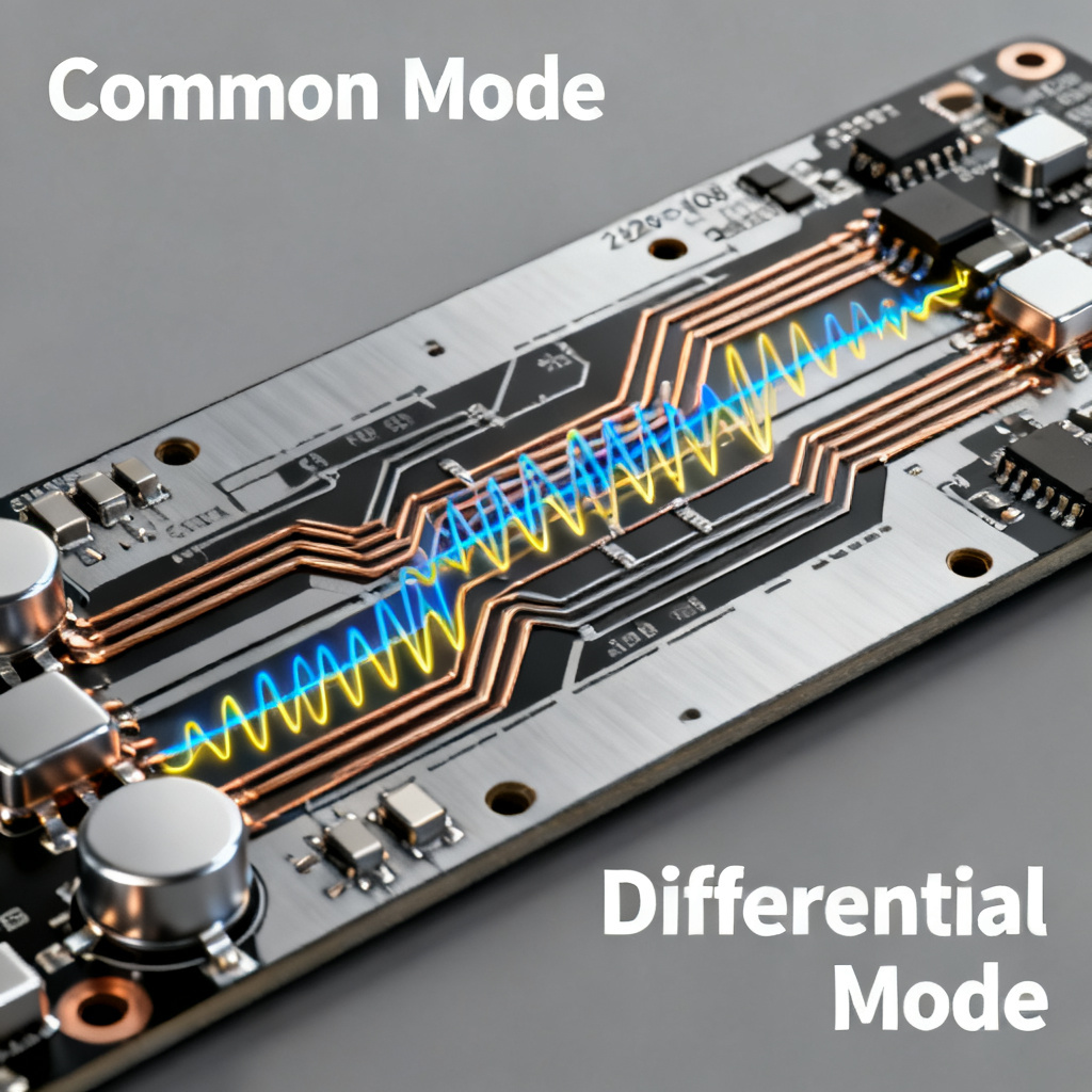
In high-speed PCB design, managing signal integrity (SI) is paramount, especially for differential pairs used in protocols like USB, HDMI, PCIe, and Ethernet. One of the most critical yet often misunderstood phenomena is reflection in transmission lines, specifically the distinction between common mode and differential mode. While differential signaling inherently offers noise immunity, reflections can degrade both the differential and common-mode signals, leading to timing errors, electromagnetic interference (EMI), and system failure.
This Pillar Content provides an exhaustive, expert-level exploration of reflection in differential pairs, focusing on the distinct behaviors of Common Mode and Differential Mode. By synthesizing the most authoritative knowledge from leading industry sources—including high-speed design guides, academic textbooks, and professional engineering blogs—we cover the physics, impedance discontinuities, measurement techniques, and mitigation strategies. Whether you are a junior engineer or a seasoned PCB layout specialist, this guide will deepen your understanding and improve your design outcomes.
1. The Fundamentals: Differential Pairs and Transmission Line Theory for Reflection
Before diving into reflection, we must establish the foundation. A differential pair consists of two coupled transmission lines (traces) that carry equal and opposite signals. Reflection in transmission line for differential pairs originates from impedance mismatches in these paths.
- Differential Mode (Odd Mode): The signal is the voltage difference between the two traces (Vdiff = V+ – V-). The currents flow in opposite directions. This mode is the primary signal path for data.
- Common Mode (Even Mode): The signal is the average voltage of the two traces (Vcm = (V+ + V-)/2). The currents flow in the same direction. Ideally, common-mode signals are zero, but in reality, they arise from skew, driver imbalances, or external noise.
Key Characteristic Impedances
- Differential Impedance (Zdiff): The impedance seen by the differential signal. For typical high-speed interfaces, this is 100Ω (or 85Ω, 90Ω for some standards).
- Common-Mode Impedance (Zcm): The impedance seen by the common-mode signal. This is typically 25Ω (for a 100Ω differential pair, Zcm ≈ Zdiff/4, assuming loose coupling).
- Odd-Mode Impedance (Zodd): The impedance of a single trace when driven differentially. Zodd = Zdiff/2.
- Even-Mode Impedance (Zeven): The impedance of a single trace when driven in common mode. Zeven = 2 * Zcm.
Reflection Basics
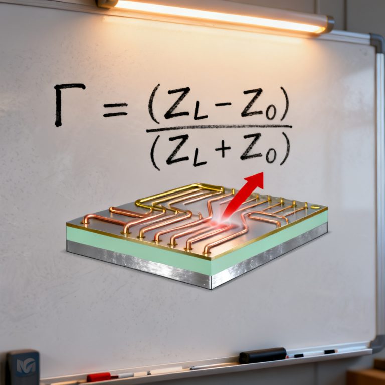
Reflection occurs when a signal encounters an impedance discontinuity (Z1 ≠ Z2). The reflection coefficient (Γ) is defined as: Γ = (Z2 – Z1) / (Z2 + Z1). For differential pairs, we must consider reflection coefficients for both differential and common modes separately.
2. Reflection in Differential Mode (Odd Mode) for High-Speed PCB
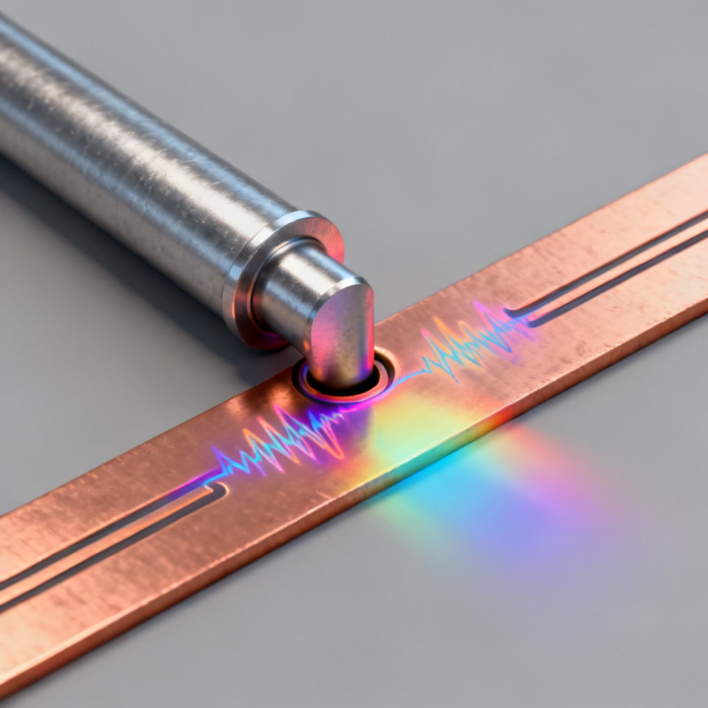
When a differential signal travels down a pair, if the differential impedance (Zdiff) is constant and matches the source and load, no reflection occurs. However, if the trace width changes, the dielectric thickness varies, or the pair encounters a via or connector, Zdiff changes. This is a primary source of reflection in transmission line for differential pairs.
Key Sources of Differential Mode Reflections
- Trace Geometry Variations: Changes in trace width, spacing, or copper thickness.
- Via Stubs and Anti-pads: Unused via stubs create capacitance, lowering Zdiff. Improper anti-pad sizing can cause impedance dips.
- Connector and Cable Interfaces: Mismatches between PCB trace impedance and connector/cable impedance.
- Bends and Corners: While 45-degree or curved bends are better, sharp 90-degree bends can cause localized impedance changes.
Behavior and Impact
- Positive Reflection (Γ > 0): Occurs when Zdiff increases (e.g., a narrow trace). The reflected signal adds to the incident signal, causing overshoot.
- Negative Reflection (Γ < 0): Occurs when Zdiff decreases (e.g., a via or stub). The reflected signal subtracts, causing undershoot.
- Impact on Eye Diagram: Differential mode reflections cause eye closure (reduced vertical and horizontal eye opening), jitter, and increased bit error rate (BER).
Measurement & Simulation
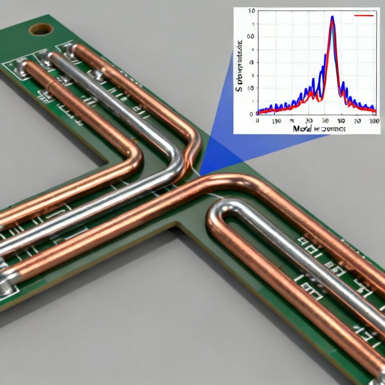
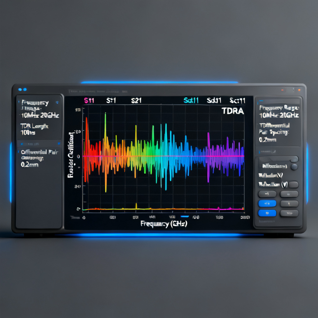
- Time Domain Reflectometry (TDR): A differential TDR (or two single-ended TDRs) can measure Zdiff along the trace. A rise or dip in the impedance plot indicates a reflection source.
- S-Parameters: Sdd11 (differential return loss) quantifies the amount of differential signal reflected back to the source. A good design targets Sdd11 < -15 dB to -20 dB across the operating frequency range.
Mitigation Strategies
- Maintain Constant Geometry: Use controlled impedance stack-ups. Keep trace width and spacing constant over the entire length.
- Optimize Vias: Use back-drilling to remove stubs. Size anti-pads to maintain Zdiff. Use smaller via pads to reduce capacitance.
- Match Connectors: Choose connectors with matched impedance (e.g., 100Ω differential). Use simulation tools to model the transition.
- Avoid Sharp Bends: Use 45-degree chamfered bends or curved traces. For critical pairs, minimize bends entirely.
3. Reflection in Common Mode (Even Mode) and Its Impact on EMI
Common-mode reflections are often more insidious than differential mode reflections because they do not directly degrade the differential signal quality—but they cause EMI and radiated emissions. Common-mode current flows in the same direction on both traces, creating a loop antenna with the ground plane. Understanding this reflection in transmission line for differential pairs is critical for compliance.
Key Sources of Common Mode Reflections
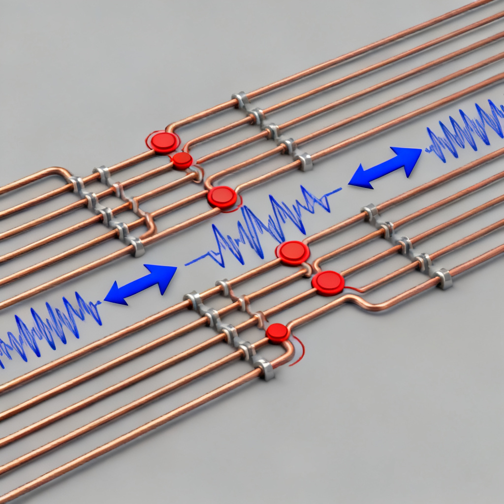
- Skew (Length Mismatch): If one trace is longer than the other, the signals arrive at different times. The receiver sees a momentary common-mode component. This skew creates a differential-to-common mode conversion.
- Driver Imbalance: Imperfect differential drivers produce a non-zero common-mode voltage.
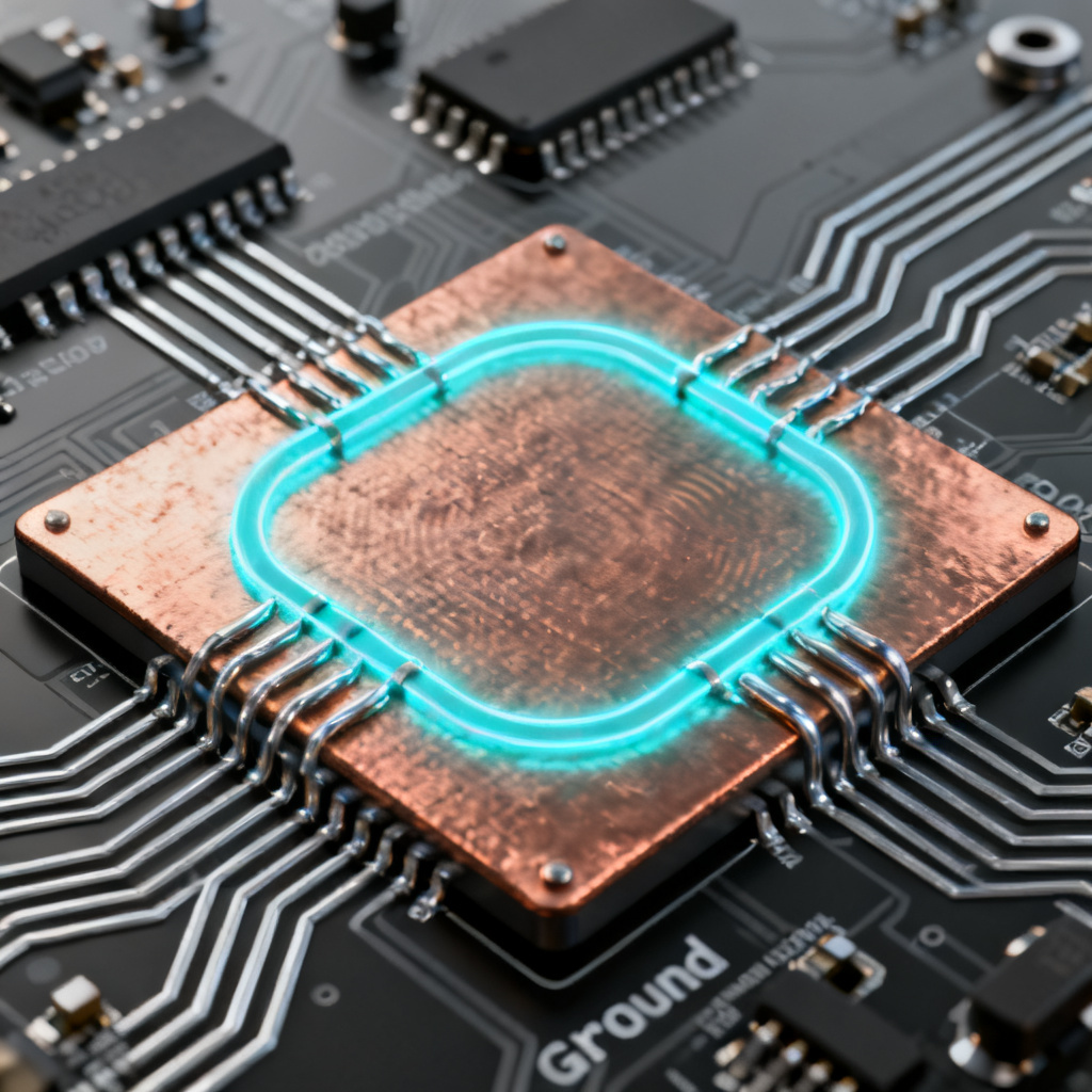
- Ground Plane Discontinuities: Slots, splits, or voids in the ground plane under the differential pair create a large common-mode impedance discontinuity.
- Coupling Variations: Changes in trace spacing (s) alter the coupling coefficient (k). When coupling changes, Zcm changes even if Zdiff is kept constant. This is a common mistake: designers focus on Zdiff but ignore Zcm.
- Stubs and Vias: The same via stubs that affect Zdiff also affect Zcm, often more severely because the common-mode signal sees a lower impedance path to ground.
Behavior and Impact
- Common-Mode Reflection Coefficient (Γcm): Γcm = (Zcm2 – Zcm1) / (Zcm2 + Zcm1).
- Mode Conversion (Scd21): This S-parameter measures how much of a differential input signal is converted to common-mode output. A high Scd21 value (e.g., > -20 dB) indicates strong common-mode reflections and EMI risk.
- Impact on EMI: Reflected common-mode currents travel back toward the source. If the source impedance is not matched to Zcm, the currents reflect again, creating a standing wave. This radiates energy, failing FCC/CE compliance tests.
Measurement & Simulation
- TDR for Common Mode: A common-mode TDR applies a step voltage to both traces simultaneously. The measured impedance is Zcm.
- Mixed-Mode S-Parameters: Scd11 (common-mode return loss) and Scd21 (mode conversion) are critical. A low Scd11 (e.g., < -10 dB) is desired. Scd21 should be as low as possible (e.g., < -30 dB).
- Near-Field Scanning: Probes can detect common-mode radiation hotspots.
Mitigation Strategies
- Match Lengths Precisely: Use serpentine routing to equalize trace lengths within 5-10 mils (or better, < 1% of the signal rise time).
- Maintain Constant Coupling: Keep trace spacing (s) constant. Avoid routing near edges or over slots. Use a solid ground plane.
- Use Common-Mode Chokes (CMC): For external cables (e.g., HDMI, USB), a CMC filters out common-mode noise by presenting a high impedance to common-mode currents and low impedance to differential currents.
- Optimize Ground Plane: Ensure a continuous, low-impedance return path. Use stitching vias near ground plane transitions.
- Control Driver Balance: Use differential drivers with low common-mode output voltage (e.g., < 50 mV).
4. The Critical Distinction: Differential vs Common Mode Reflections
| Feature | Differential Mode Reflection | Common Mode Reflection |
|---|---|---|
| Cause | Impedance mismatch in Zdiff | Impedance mismatch in Zcm |
| Primary Impact | Signal integrity (eye closure, jitter) | EMI, radiated emissions |
| Detection | Sdd11, differential TDR | Scd11, Scd21, common-mode TDR |
| Mitigation Focus | Trace geometry, vias, connectors | Length matching, coupling, ground plane |
| Example Failure | Data errors at receiver | FCC/CE compliance failure |
The Interplay
It is crucial to understand that these two modes are not independent. A discontinuity that causes a differential reflection (e.g., a via) also causes a common-mode reflection. Furthermore, skew converts differential energy into common-mode energy, which then reflects and radiates. Conversely, a common-mode noise source can couple into the differential pair, causing differential noise. This interplay is central to reflection in transmission line for differential pairs.
Design Rule of Thumb
- For SI: Focus on maintaining Zdiff (constant width/spacing, optimized vias).
- For EMI: Focus on minimizing common-mode current (length matching, constant coupling, solid ground).
- The Golden Rule: A perfectly balanced differential pair with zero skew and constant coupling will have minimal common-mode reflections, even if Zdiff is slightly off.
5. Advanced Considerations and Design Techniques for Reflection in Transmission Line for Differential Pairs
5.1 The Role of Coupling (k)
Coupling between traces affects both Zdiff and Zcm. Loose coupling (large spacing) makes Zdiff ≈ 2 * Z0 (where Z0 is the single-ended impedance). Tight coupling (small spacing) lowers Zdiff and raises Zcm. For high-speed designs, tight coupling is often preferred because it reduces common-mode susceptibility and makes the pair less sensitive to ground plane discontinuities. However, it makes impedance control more challenging.
5.2 Reflection from Discontinuities in Differential Pairs (The “Odd-Even Mode” Approach)
A more rigorous analysis uses odd and even modes. For any discontinuity:
- The odd-mode component (Vodd) sees the odd-mode impedance (Zodd).
- The even-mode component (Veven) sees the even-mode impedance (Zeven).
If the discontinuity is symmetric (both traces see the same change), only the even mode (common mode) is affected. If the discontinuity is asymmetric (e.g., a stub on one trace only), both odd and even modes are affected, causing mode conversion.
5.3 Simulation-Driven Design
Modern tools (e.g., Ansys HFSS, Keysight ADS, CST) can simulate mixed-mode S-parameters and TDR responses. Always simulate the entire channel—from driver to receiver—including vias, connectors, and any length mismatch. Look for:
- Sdd11 < -15 dB (preferably < -20 dB)
- Scd21 < -30 dB (preferably < -40 dB)
- Zdiff within ±10% of target (e.g., 90-110Ω for 100Ω target)
- Zcm stable (e.g., 20-30Ω)
5.4 Practical PCB Layout Guidelines for High-Speed Differential Pairs
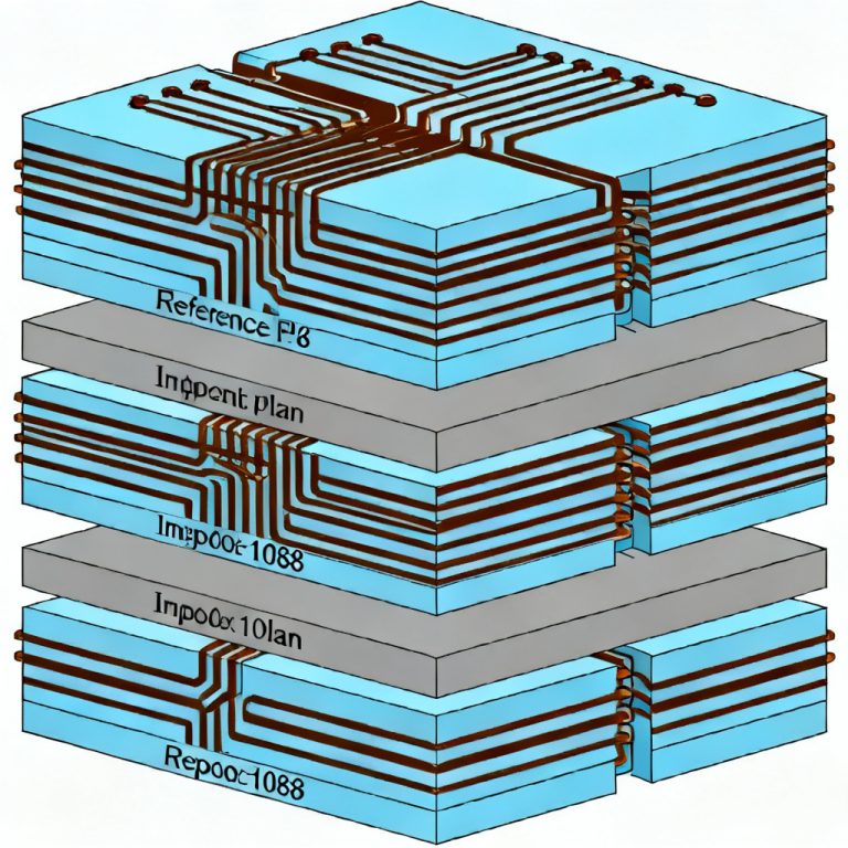
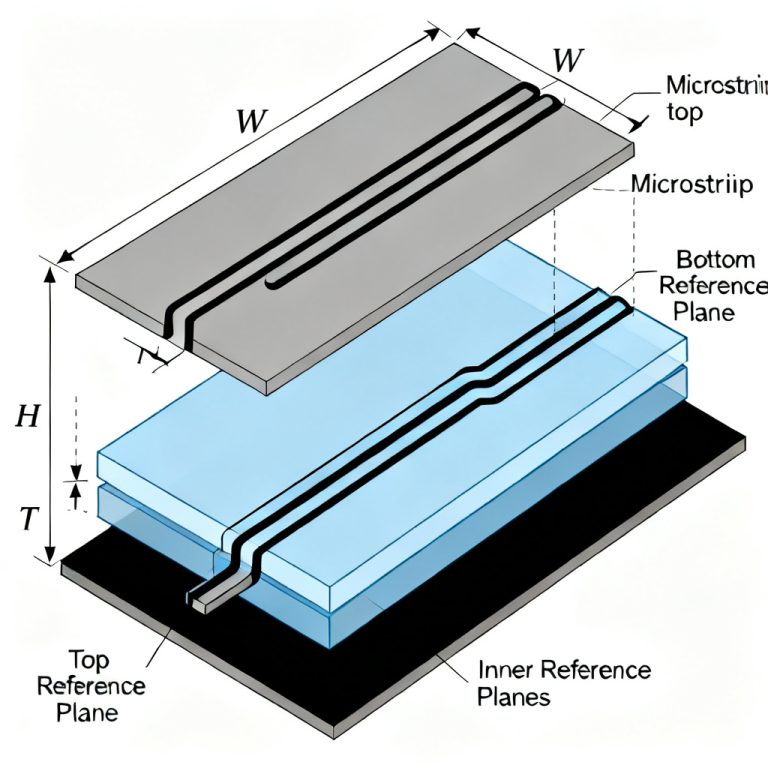
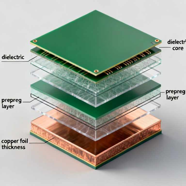
- Layer Stack-Up: Use a symmetric stack-up with reference planes (GND or VCC) adjacent to the signal layer. Avoid routing over gaps.
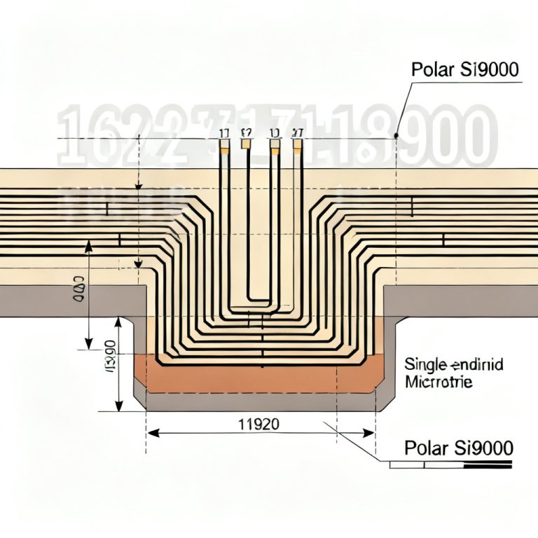
- Trace Geometry: Use a constant trace width (w) and spacing (s). For a 100Ω differential pair on a standard FR4 stack-up, typical values are w=5-7 mils, s=5-10 mils (tight coupling).
- Length Matching: Match lengths within 5-10 mils. Use “accordion” or “trombone” serpentine patterns, not “hairpin” bends.
- Via Design: Use back-drilling for high-speed signals (>5 Gbps). Place ground vias near signal vias to provide a return path.
- Connector Transitions: Simulate the connector footprint. Often, a “neck-down” or pad size adjustment is needed to maintain impedance.
- Guard Traces: Avoid using guard traces (grounded copper between pairs) unless absolutely necessary, as they can couple to the pair and alter Zdiff. If used, ensure they are grounded with vias every λ/10.
6. Conclusion: Achieving Signal Integrity and EMI Compliance
Reflection in differential pairs is a dual-mode problem. While differential mode reflections directly impact signal integrity (eye closure, jitter), common-mode reflections are the primary cause of EMI. A successful high-speed PCB design must address both.
Key Takeaways
- Design for Zdiff: Use controlled impedance stack-ups, constant geometry, and optimized vias.
- Design for Zcm: Match trace lengths precisely, maintain constant coupling, and ensure a solid ground plane.
- Simulate Mixed-Mode S-Parameters: Don’t just check Sdd11; check Scd21 and Scd11.
- Measure with TDR: Validate your design with differential and common-mode TDR measurements.
- Balance is Everything: A perfectly balanced differential pair is the most robust against both SI and EMI issues.
By mastering the concepts of common-mode vs. differential mode reflections, you will move beyond basic routing rules and achieve first-pass success in your high-speed PCB designs. Whether you are designing a 10 Gbps backplane or a simple USB 3.0 interface, this knowledge is the foundation of robust, reliable, and compliant products.
This content is intended as a comprehensive educational resource. For specific design assistance, please contact our engineering team. We specialize in high-speed PCB fabrication and assembly, ensuring your designs meet the most stringent signal integrity requirements.
FAQ: Reflection in Transmission Line for Differential Pairs
What is the main difference between common mode and differential mode reflection?
Differential mode reflection affects signal integrity by causing eye closure and jitter, while common mode reflection primarily causes EMI and radiated emissions. Both are types of reflection in transmission line for differential pairs.
How does skew cause common mode reflection?
Skew (length mismatch) converts differential energy into common-mode energy, which then reflects and radiates. This mode conversion is a key source of reflection in transmission line for differential pairs.
What are the best tools to measure reflection in differential pairs?
Time Domain Reflectometry (TDR) and mixed-mode S-parameters (Sdd11, Scd21) are the standard tools for analyzing reflection in transmission line for differential pairs.
Can a perfectly matched differential pair still have common mode reflection?
Yes, if ground plane discontinuities or coupling variations exist, common mode reflection can occur even if Zdiff is perfectly matched. This highlights the need to address both modes in reflection in transmission line for differential pairs.
How do I reduce common mode reflection in my PCB design?
Match trace lengths precisely, maintain constant coupling, use a solid ground plane, and consider common-mode chokes for external cables. These steps directly mitigate reflection in transmission line for differential pairs.