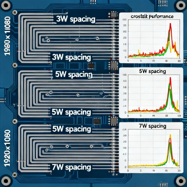
In high-speed PCB design, the eye diagram is the most powerful tool for evaluating signal integrity. This page explains why the eye diagram PCB at the receiver looks fundamentally different from the transmitter, and how to interpret these differences for reliable data transmission.
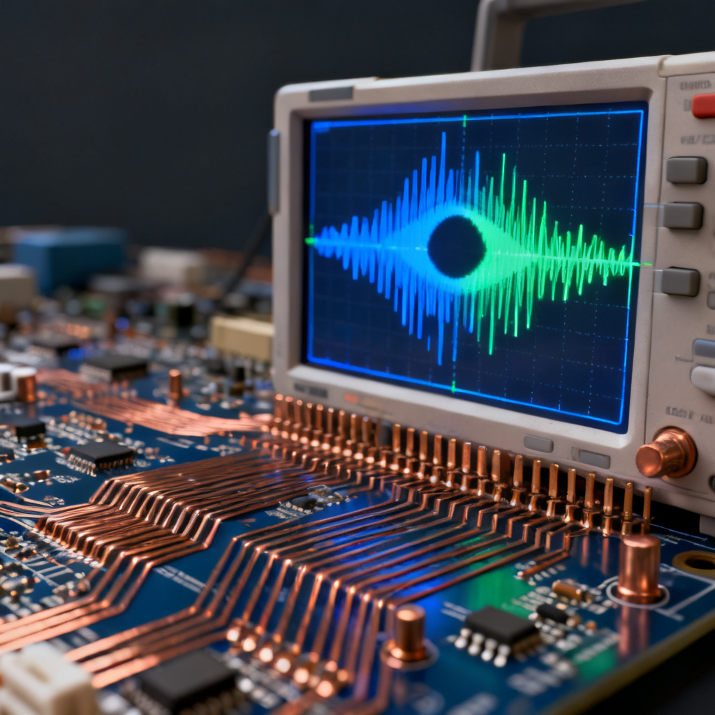
What Is an Eye Diagram PCB?
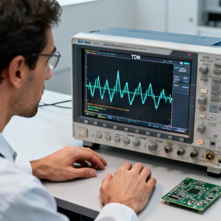
An eye diagram PCB is created by overlaying multiple transitions of a digital signal on an oscilloscope, forming an “eye” pattern. The wider and clearer the eye opening, the better the signal quality. Key parameters include eye height, eye width, jitter, and rise/fall times.
Key Parameters of Eye Diagram PCB
- Eye Height: Vertical opening, indicating noise margin.
- Eye Width: Horizontal opening, indicating timing margin.
- Jitter: Horizontal dispersion of edges, representing timing uncertainty.
- Rise/Fall Times: Speed of signal transitions.
Transmitter Eye Diagram PCB: The Ideal Start
At the transmitter, the eye diagram PCB is generated directly from the output driver. This is the cleanest version of the signal, with maximum amplitude and minimal distortion.
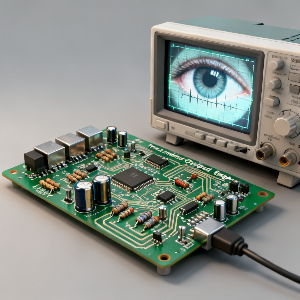
- Wide Eye Opening: Large and well-defined due to minimal channel loss.
- Low Jitter: Primarily deterministic from internal clock jitter, typically very low.
- Sharp Transitions: Fast rise/fall times, often under 100 ps for high-speed signals like PCIe 5.0.
- Minimal Noise: High signal-to-noise ratio (SNR) because the driver is directly connected.
Why It Looks Different from RX: The TX eye is a “before” picture, showing what the signal ideally should be, without channel degradation.
Receiver Eye Diagram PCB: The Reality After the Channel
At the receiver, the eye diagram PCB has passed through the entire PCB channel, including traces, vias, and connectors. This channel acts as a low-pass filter, attenuating high-frequency components.
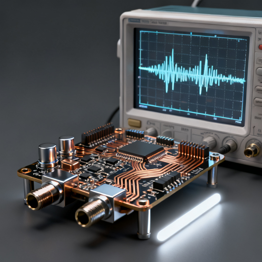
- Narrower Eye Opening: Eye height and width are significantly reduced due to attenuation and reflections.
- Increased Jitter: Combination of deterministic jitter (ISI, duty cycle distortion) and random jitter (thermal noise).
- Slower Transitions: High-frequency content is lost, lengthening rise/fall times.
- Noise and Distortion: Channel-induced noise from impedance mismatches and crosstalk.
Why It Looks Different from TX: The RX eye is an “after” picture, revealing the cumulative effect of the channel. The difference between TX and RX is a direct measure of channel loss and signal integrity degradation.
Why They Look Different: The Physics of Signal Degradation
The primary reason for the visual difference between TX and RX eye diagram PCB measurements is channel loss. Here’s a breakdown of the key factors:
1. Attenuation and Skin Effect
At high frequencies (e.g., 10 GHz and above), skin effect increases resistance, and dielectric losses in PCB materials (like FR-4) absorb high-frequency energy. This rounds edges and reduces eye height.
2. Inter-Symbol Interference (ISI)
When the channel cannot settle between bits, energy from one symbol bleeds into the next. ISI closes the eye horizontally and vertically, creating multiple “ghost” edges in the RX eye.
3. Reflections and Impedance Mismatches
Impedance discontinuities (e.g., at vias, connectors, or trace bends) cause signal reflections that add jitter and amplitude distortion at RX, invisible at TX.
4. Crosstalk
Signals on adjacent traces couple capacitively and inductively, adding noise that further closes the RX eye. At TX, this coupling is negligible due to strong drivers.
5. Power Supply Noise and Ground Bounce
At RX, power supply noise adds random jitter. At TX, the driver’s isolation typically keeps noise lower.
How to Interpret the Differences for High-Speed PCB Design
Understanding these differences is critical for troubleshooting and optimization of your eye diagram PCB measurements:
| Parameter | Transmitter Eye Diagram PCB | Receiver Eye Diagram PCB |
|---|---|---|
| Eye Height | Large (e.g., 800 mV) | Reduced (e.g., 200 mV) |
| Eye Width | Wide | Narrowed (e.g., 30% reduction) |
| Jitter | Low (e.g., 5 ps) | High (e.g., 25 ps) |
| Rise/Fall Times | Fast (<100 ps) | Slower |
| Noise | Minimal | Significant (crosstalk, reflections) |
If the TX Eye Is Good but the RX Eye Is Closed
Cause: Excessive channel loss, severe reflections, or high crosstalk. Solution: Use lower-loss PCB materials (e.g., Rogers 4350B or Megtron 6), reduce trace length, add equalization (CTLE or DFE) at the receiver, or implement pre-emphasis/de-emphasis at the transmitter.
If Both TX and RX Eyes Are Poor
Cause: The transmitter driver itself may be faulty (e.g., weak driver, excessive internal jitter). Solution: Check the driver’s output impedance, power supply, and clock jitter.
If the RX Eye Shows Significant Vertical Closure but Horizontal Opening Is OK
Cause: Attenuation is the dominant issue. Solution: Increase driver swing or use a receiver with higher sensitivity.
If the RX Eye Shows Wide Horizontal Jitter but Good Vertical Opening
Cause: ISI or reflections are dominant. Solution: Add equalization, optimize termination, or reduce stub lengths.
Practical Measurement Tips for Engineers
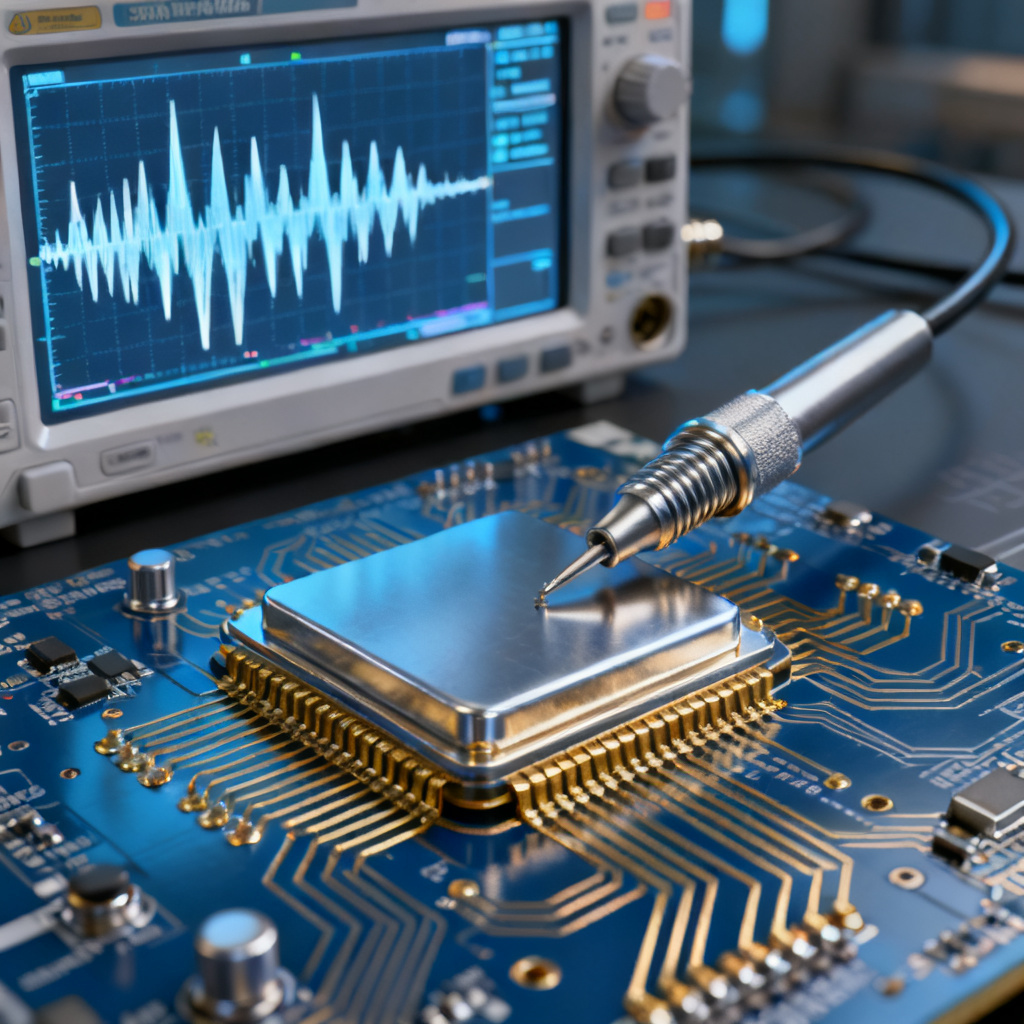
- Use a High-Bandwidth Oscilloscope: Bandwidth should be at least 3x the signal’s fundamental frequency (e.g., 12 GHz for a 4 GHz signal).
- Minimize Probe Loading: Use active differential probes with low capacitance (<0.5 pF) to avoid distorting the RX eye.
- Measure at the Receiver Pin: Measure as close to the receiver input as possible, ideally at the BGA ball or connector pin.
- Use a Pattern Generator: Use a PRBS (Pseudo-Random Bit Sequence) pattern to mimic real data traffic.
- Compare with Simulation: Use tools like HyperLynx or ADS to predict the RX eye and validate your design.
Case Study: A High-Speed PCB with 10 Gbps Differential Pair
Consider a 10 Gbps differential pair on standard FR-4 with a trace length of 12 inches.
- TX Eye: Eye height of 800 mV, jitter of only 5 ps.
- RX Eye: Eye height of 200 mV, jitter of 25 ps, eye width reduced by 30%.
Analysis: Channel loss is approximately 15 dB at 5 GHz. The RX eye is still open enough for a receiver with CTLE to recover data, but any additional length or impedance mismatch would close it completely.
Action: Use a low-loss material (e.g., Megtron 6) and add a 2-tap DFE in the receiver. The simulated RX eye improves to 400 mV eye height and 12 ps jitter.
Conclusion
The eye diagram PCB at the transmitter and receiver are two different snapshots of the same signal, separated by the physical channel. The TX eye represents the ideal signal, while the RX eye reveals the harsh reality of loss, reflections, and noise. For high-speed PCB design, the difference between these two eyes is your most valuable metric—it quantifies the channel’s impact and guides your choices in materials, equalization, and layout.
At [Your Company Name], we specialize in manufacturing high-speed PCBs that minimize this difference. Our advanced materials, optimized stackups, and rigorous signal integrity testing ensure that your receiver eye stays open, even at 25+ Gbps. Contact us for a free design review and simulation.