Ground bounce caused by poor return path PCB design is a critical signal integrity issue in high-speed digital systems. This phenomenon degrades noise margins, causes false logic switching, and limits system performance. Understanding its mechanisms and applying proven mitigation strategies is essential for reliable high-speed PCB design and manufacturing.
Understanding the Mechanism of Ground Bounce Caused by Poor Return Path
The Physics of the Return Path
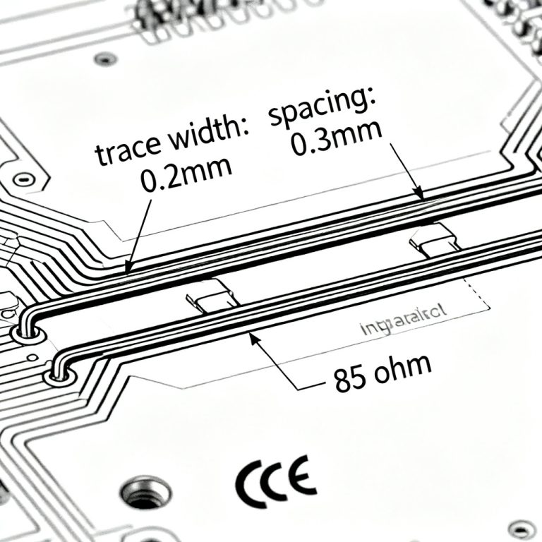
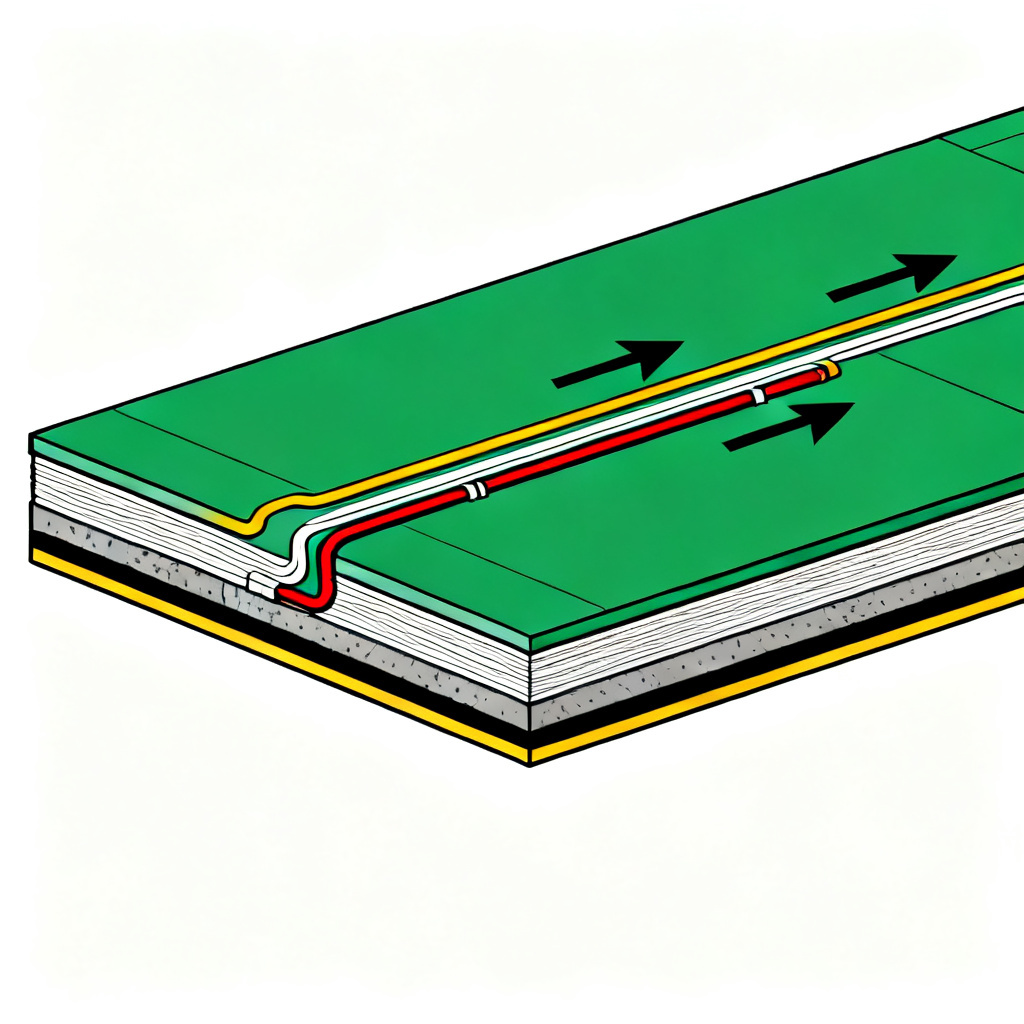
Every signal is a loop. A digital signal does not travel solely on the trace; it requires a return current to complete the circuit. At high frequencies (typically above 50-100 MHz), the return current takes the path of least inductance, which is the plane directly beneath the signal trace (the reference plane). This is due to the electromagnetic field coupling between the trace and the plane. The return current flows as a “mirror image” on the reference plane, hugging the trace’s path. The return current path is defined by the distribution of the electromagnetic field. At high frequencies, the skin effect and proximity effect force the return current into a narrow band directly under the trace. This creates a transmission line structure (microstrip or stripline). If this reference plane is broken—by a split, a slot, or a missing via—the return current is forced to find a longer, higher-inductance path.
What is Ground Bounce?
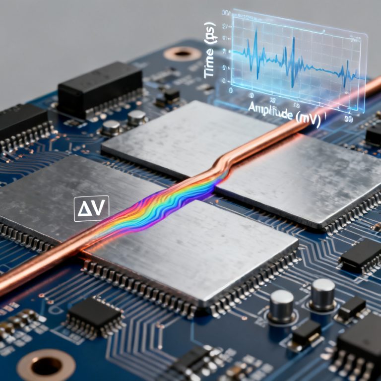
Ground bounce is a voltage fluctuation on the ground (or power) reference plane relative to the ideal 0V reference. It is a specific type of Simultaneous Switching Noise (SSN). When multiple outputs switch simultaneously, a large transient current (di/dt) flows through the power delivery network (PDN). This current, combined with the parasitic inductance (L) of the package, bond wires, and the PCB’s return path, induces a voltage spike according to the fundamental law: V = L * (di/dt). Ground bounce is often measured as the voltage difference between the internal ground of a chip (e.g., an FPGA or ASIC) and the external PCB ground. A high di/dt, coupled with a high loop inductance from a poor return path, creates a significant voltage spike. This spike can cause the output driver to produce a false logic low (if the ground reference rises above the input threshold) or a false logic high (if the ground drops below the threshold). It is not a “noise” in the traditional sense but a shift in the reference voltage.
The Role of Return Path Discontinuity (RPD)
A Return Path Discontinuity (RPD) is the primary trigger for ground bounce in PCB layout. When a signal crosses a split in the ground plane, a slot in the plane, or changes reference planes (e.g., from ground to power) without a stitching via, the return current cannot follow its ideal low-inductance path. The forced detour creates a large current loop. The area of this loop directly increases the loop inductance. The equation V = L * (di/dt) now has a much larger L. This higher inductance amplifies the ground bounce voltage. For example, a signal crossing a slot in a ground plane might create a loop area 10x larger than the ideal path, leading to a 10x increase in ground bounce amplitude. This manifests as ringing, overshoot, undershoot, and crosstalk on the victim signal.
Key Terminology
- Return Path Discontinuity (RPD): Any break or interruption in the continuous reference plane that forces the return current to take a longer, higher-inductance path.
- Simultaneous Switching Noise (SSN): Noise generated on the power or ground planes when multiple output drivers switch states simultaneously, causing a transient current surge.
- Loop Inductance: The total inductance of the signal path including both the forward trace and the return path; minimizing loop area reduces this inductance.
- Stitching Via: A via that connects two reference planes (e.g., ground to ground) to provide a low-inductance path for return currents when a signal changes layers.
- Power Delivery Network (PDN): The entire system of planes, vias, and decoupling capacitors that delivers stable power to ICs; its impedance directly affects ground bounce amplitude.
Quantifying the Impact of Poor Return Paths on Ground Bounce
From Mechanism to Failure
Ground bounce caused by poor return path directly translates into design failures. A 0.5V ground bounce on a 3.3V logic family can cause a low-to-high transition if the input threshold is 0.8V. This is the most common failure mode. Ground bounce modulates the timing of clock and data signals, increasing total jitter and reducing the timing margin. The large current loop created by an RPD acts as an efficient antenna. The high di/dt in this loop generates strong electromagnetic interference (EMI), potentially failing FCC or CE compliance tests. The effective noise margin of the system shrinks, making the design sensitive to other noise sources like crosstalk. The severity of ground bounce is directly proportional to the number of simultaneously switching outputs (SSO), the switching speed (edge rate, tr/tf), and the inductance of the complete loop (package + PCB). A high-speed FPGA with 100 I/Os switching simultaneously can generate ground bounce exceeding 1V if the return path is not optimized.
Measuring Ground Bounce in Simulation and Practice
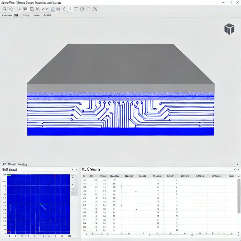
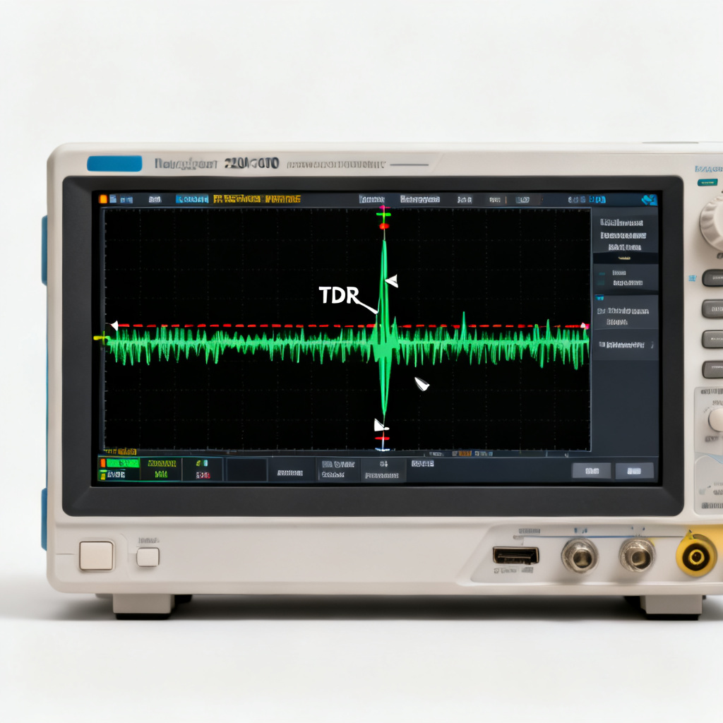
Designers can quantify ground bounce using field solvers (e.g., Ansys SIwave, CST) to extract the PDN impedance (Z) and loop inductance of the return path. A high impedance peak at the switching frequency indicates a problem. Time-Domain Reflectometry (TDR) shows the impedance discontinuity caused by a slot in the plane; the impedance spike confirms the RPD. Oscilloscope measurement probing the ground pin of an IC relative to a local, clean ground reference point reveals the ground bounce waveform.
Comparison: Ideal vs. Poor Return Path Performance
| Parameter | Ideal Return Path Design | Poor Return Path Design |
|---|---|---|
| Loop Area | Minimal (trace width × dielectric thickness) | Large (10x or more) |
| Loop Inductance | Low (nH range) | High (10s of nH) |
| Ground Bounce Amplitude | < 0.1V | 0.5V – 1.0V+ |
| EMI Emissions | Low (passes FCC/CE) | High (fails compliance) |
| Timing Margin | Robust | Reduced (jitter increase) |
As the table shows, ground bounce caused by poor return path is significantly worse across all key performance metrics. Our high-speed PCB manufacturing services specialize in optimizing return paths to ensure your design achieves ideal performance.
Mitigation Strategies for Ground Bounce Caused by Poor Return Path
Design for a Continuous Return Path
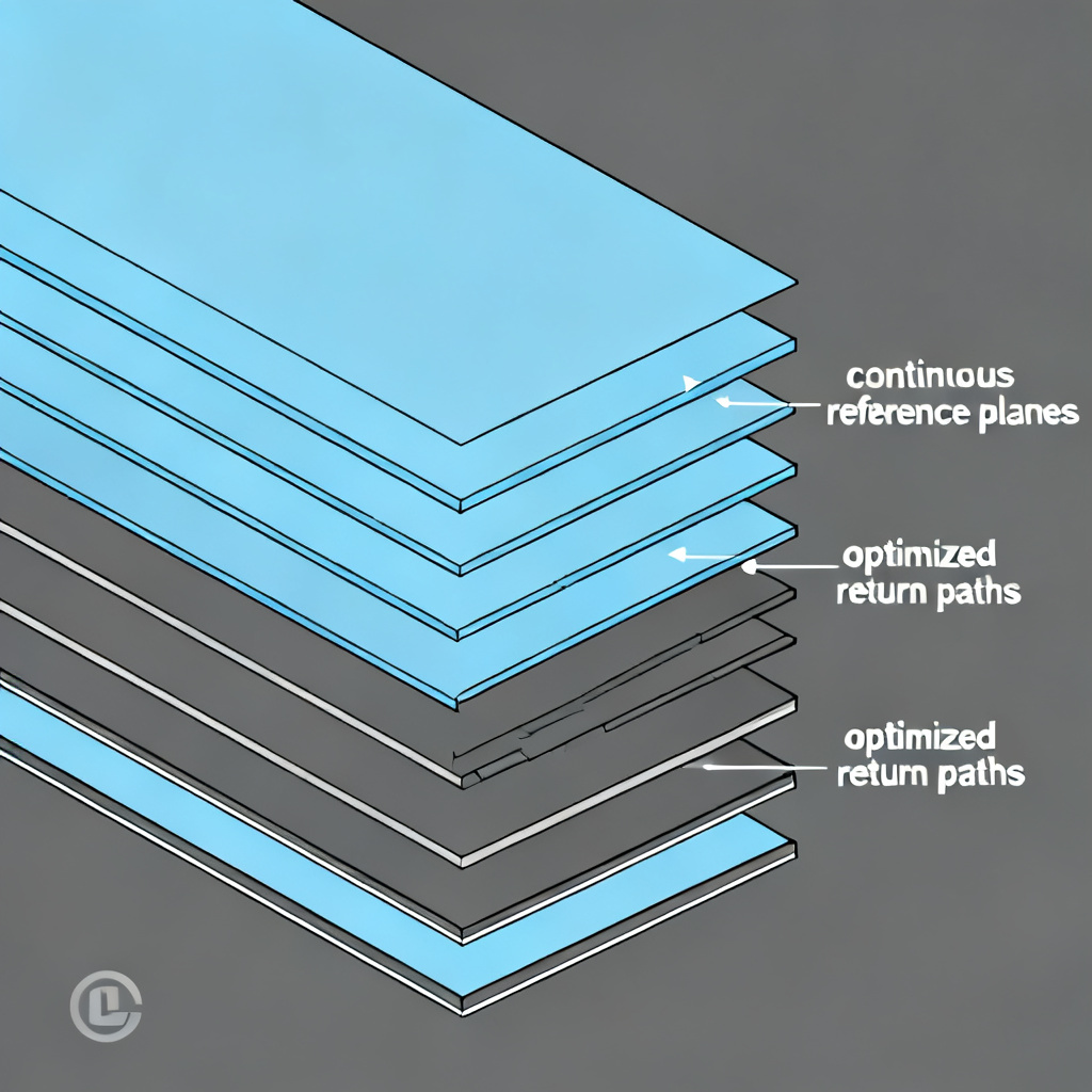
The golden rule: Never route a high-speed signal over a split in the reference plane. Use solid ground and power planes. Dedicate at least one entire layer to a solid ground plane (GND) and one to a power plane (VCC). Do not route signals across slots created for different power domains. Avoid anti-pads for through-hole connectors. When routing signals near connectors, ensure the anti-pad (the clearance hole around a via) does not cut through the return path of a nearby signal. Use ground vias adjacent to signal vias. The return path must be as wide and as short as possible. A continuous copper plane is the ideal low-inductance path. Any break forces the current to flow around it, increasing inductance.
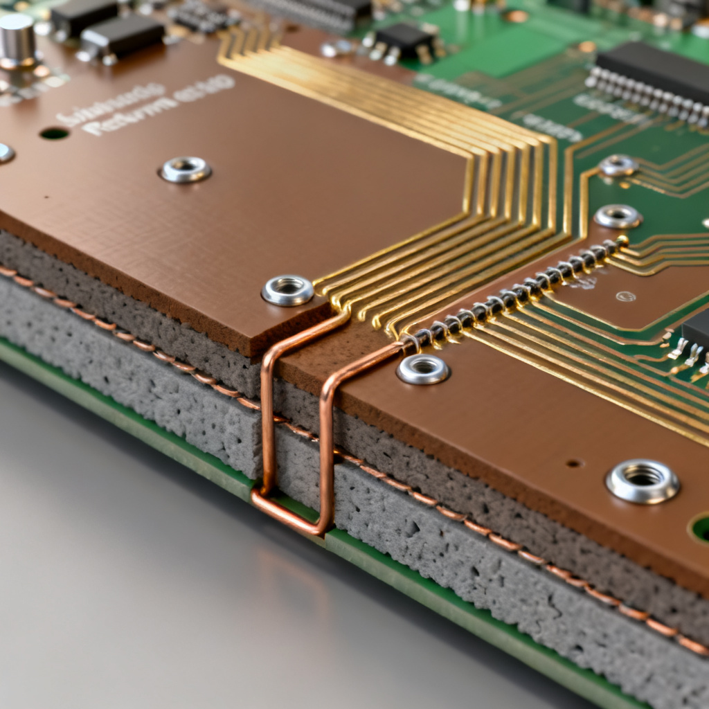
Stitching Vias for Layer Transitions
When a signal changes from one reference plane to another (e.g., from a ground plane layer to a power plane layer), the return current must also change planes. Place a stitching via—a ground via (connecting to GND) or a decoupling capacitor (if transitioning between GND and VCC)—as close as possible (within 50 mils) to the signal via. The stitching via provides a low-inductance path for the return current to jump from the original reference plane to the new one. Without it, the return current must travel a long distance through the plane capacitance or through a high-inductance path, creating a large loop. For every signal via that changes layers, there must be a corresponding ground via within a few millimeters. This is non-negotiable for signals above 1 Gbps.
Managing Simultaneous Switching Noise (SSN)
Reduce di/dt by using slower edge rates (slew rate control) on output drivers where timing allows. A slower edge reduces the transient current. Distribute switching events by avoiding switching all outputs at the exact same clock edge; use staggered switching or output enable controls. Use on-die decoupling—modern high-speed ICs have on-chip decoupling capacitors; ensure your BOM specifies parts with adequate on-die capacitance. Optimize PDN impedance by using multiple, low-ESR/ESL decoupling capacitors (e.g., 0.1µF, 1µF, 10µF) placed as close to the IC power pins as possible. The goal is to keep the PDN impedance below a target value (e.g., < 0.1 Ohm) across the frequency range of interest. Ground bounce is a PDN problem first. A low-impedance PDN with a dense array of decoupling capacitors directly under the IC (on the backside of the PCB) is the most effective mitigation.
Advanced Layout Techniques
For high-speed differential signals (e.g., USB, HDMI, PCIe), the return path is inherently controlled. The signals are referenced to each other, and the ground plane provides a secondary return. Ensure the differential pair is tightly coupled and the ground plane is continuous. Guard traces and ground fills can provide a partial return path if the main plane is interrupted, though this is a secondary solution. Via fencing—surrounding a group of high-speed vias with a “fence” of ground vias—creates a coaxial-like structure, reducing crosstalk and controlling the return path.
Case Study: Ground Bounce Caused by Poor Return Path and Its Fix
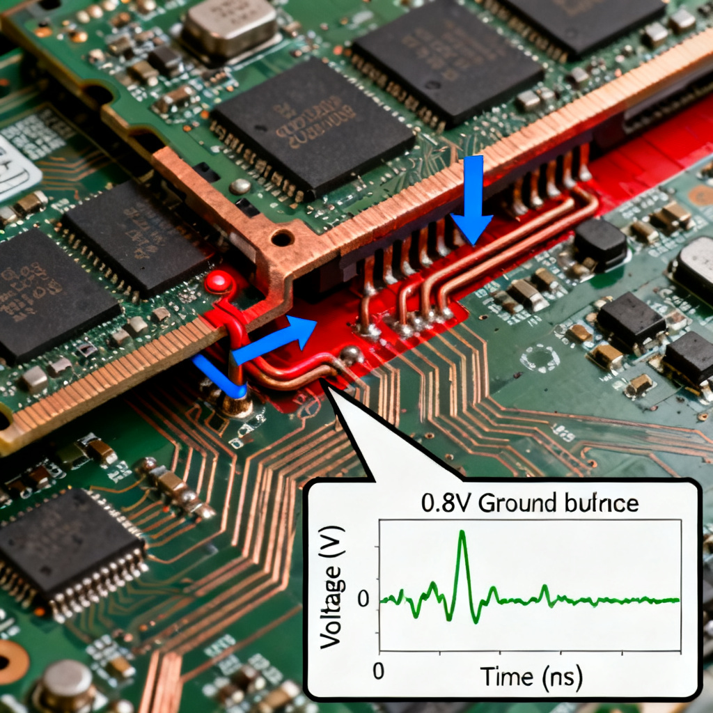
Scenario: A 4-layer PCB with a 1.8V DDR3 memory interface. The top layer (signal) routes data lines. Layer 2 is a solid GND plane. Layer 3 is a 1.8V power plane. Layer 4 is a secondary signal layer.
Problem: A data line on Layer 4 transitions to a via on Layer 1 to connect to the memory controller. The via passes through the GND plane (Layer 2) and the 1.8V plane (Layer 3). No stitching via is placed. The return current, which was flowing on the GND plane, must now find a path. It travels through the capacitance between the GND and 1.8V planes (a slow, high-inductance path) and then back to the IC. This creates a 0.8V ground bounce on the 1.8V plane, causing false reads on the memory bus.
Solution: A 0.1µF decoupling capacitor is placed between the 1.8V plane and GND, within 30 mils of the signal via. This capacitor acts as a low-impedance AC short, providing a stitching path for the return current. The ground bounce drops to 0.15V, and the memory interface operates reliably.
This case demonstrates that ground bounce caused by poor return path is both predictable and preventable with proper design techniques.
Best Practices for Your PCB Design to Prevent Ground Bounce
Ground bounce caused by poor return path design is a critical signal integrity issue that can derail high-speed designs. By understanding the electromagnetic mechanisms and applying these mitigation strategies, you can ensure robust, reliable performance.
Final Checklist for High-Speed PCB Layout
- Maintain Solid Reference Planes: Never route high-speed signals over splits or slots.
- Use Stitching Vias: Every signal via that changes reference planes needs a ground via nearby.
- Minimize Loop Area: The return path loop must be as small as possible (ideally, the trace width × dielectric thickness).
- Optimize PDN: Use a dense array of decoupling capacitors directly under the IC.
- Control Edge Rates: Use the slowest edge rate that meets timing requirements.
By partnering with a PCB manufacturer that understands these high-speed design principles, you can avoid costly prototype spins and achieve first-pass success in your high-speed digital products. Contact our engineering team today for a design review or to discuss your next high-speed PCB project. We specialize in manufacturing PCBs with optimized return paths to minimize ground bounce and maximize signal integrity.
FAQ: Ground Bounce and Return Path Design
What is ground bounce caused by poor return path PCB design?
Ground bounce caused by poor return path PCB design is a voltage fluctuation on the ground or power reference plane resulting from a discontinuous or high-inductance return path for high-speed signals. It is a form of Simultaneous Switching Noise (SSN) that can cause false logic transitions and signal integrity degradation.
How does a poor return path cause ground bounce?
A poor return path, such as a split in the ground plane or missing stitching vias, forces the return current to take a longer, higher-inductance path. This increases loop inductance (L), and when combined with high transient current (di/dt), produces a larger voltage spike (V = L * di/dt) known as ground bounce.
What are the best mitigation strategies for ground bounce in high-speed PCBs?
Key mitigation strategies include maintaining continuous reference planes, using stitching vias for layer transitions, optimizing the Power Delivery Network (PDN) with decoupling capacitors, controlling edge rates, and minimizing loop area. These techniques directly address ground bounce caused by poor return path design.
Can ground bounce be simulated before PCB fabrication?
Yes, ground bounce can be simulated using field solvers like Ansys SIwave or CST to extract PDN impedance and loop inductance. Time-Domain Reflectometry (TDR) can also identify return path discontinuities. Our high-speed PCB manufacturing services can help validate your design before production.
What is the role of stitching vias in reducing ground bounce?
Stitching vias provide a low-inductance path for return currents when a signal changes reference planes. By placing a ground via near the signal via, the return current can transfer efficiently, reducing loop inductance and minimizing ground bounce caused by poor return path transitions.