Understanding how board thickness affects crosstalk in high speed PCB design is critical for signal integrity at 10Gbps+. This pillar content reveals the hidden electromagnetic trade-offs between stackup thickness, impedance control, and EMI, providing expert guidance for your next high-speed project.
Fundamental Physics of Board Thickness and Crosstalk in High Speed PCB
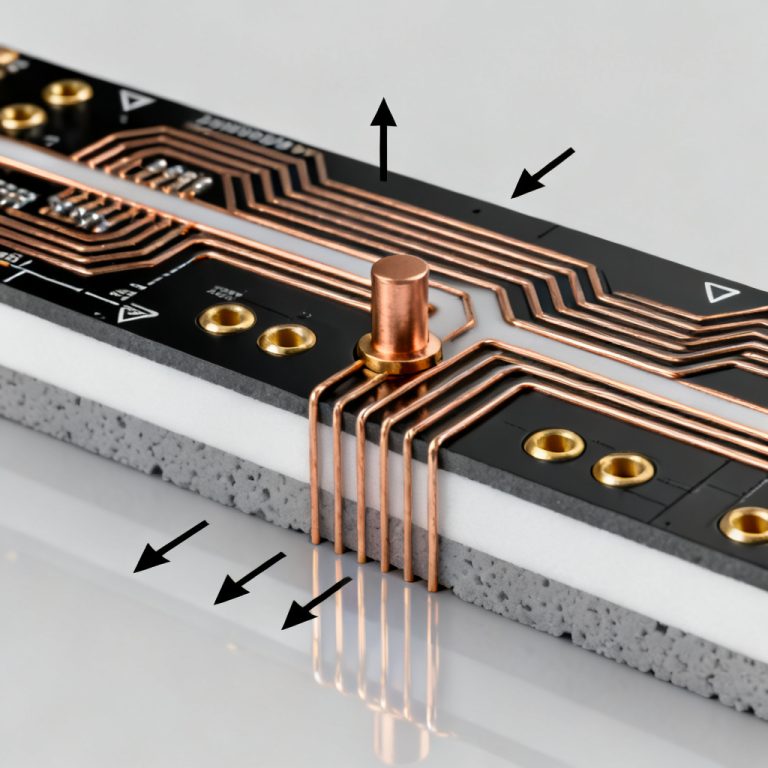
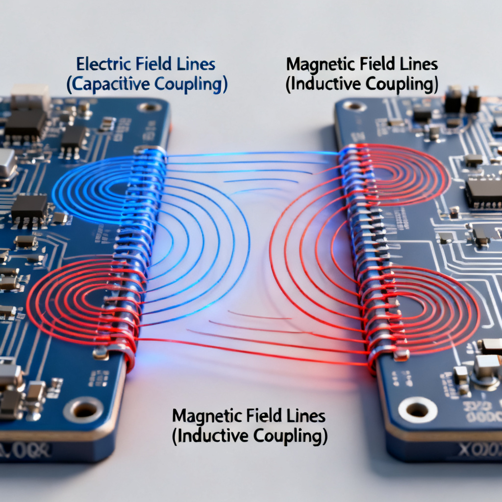
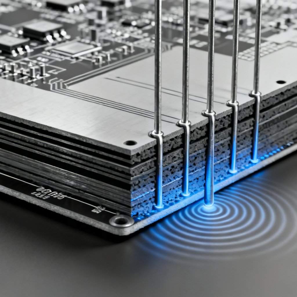
Board thickness affects crosstalk in high speed PCB design through two core electromagnetic mechanisms: capacitive coupling (electric field) and inductive coupling (magnetic field). The return current path, determined by dielectric thickness between trace and reference plane, is the key variable.
Capacitive and Inductive Coupling in High Speed PCB
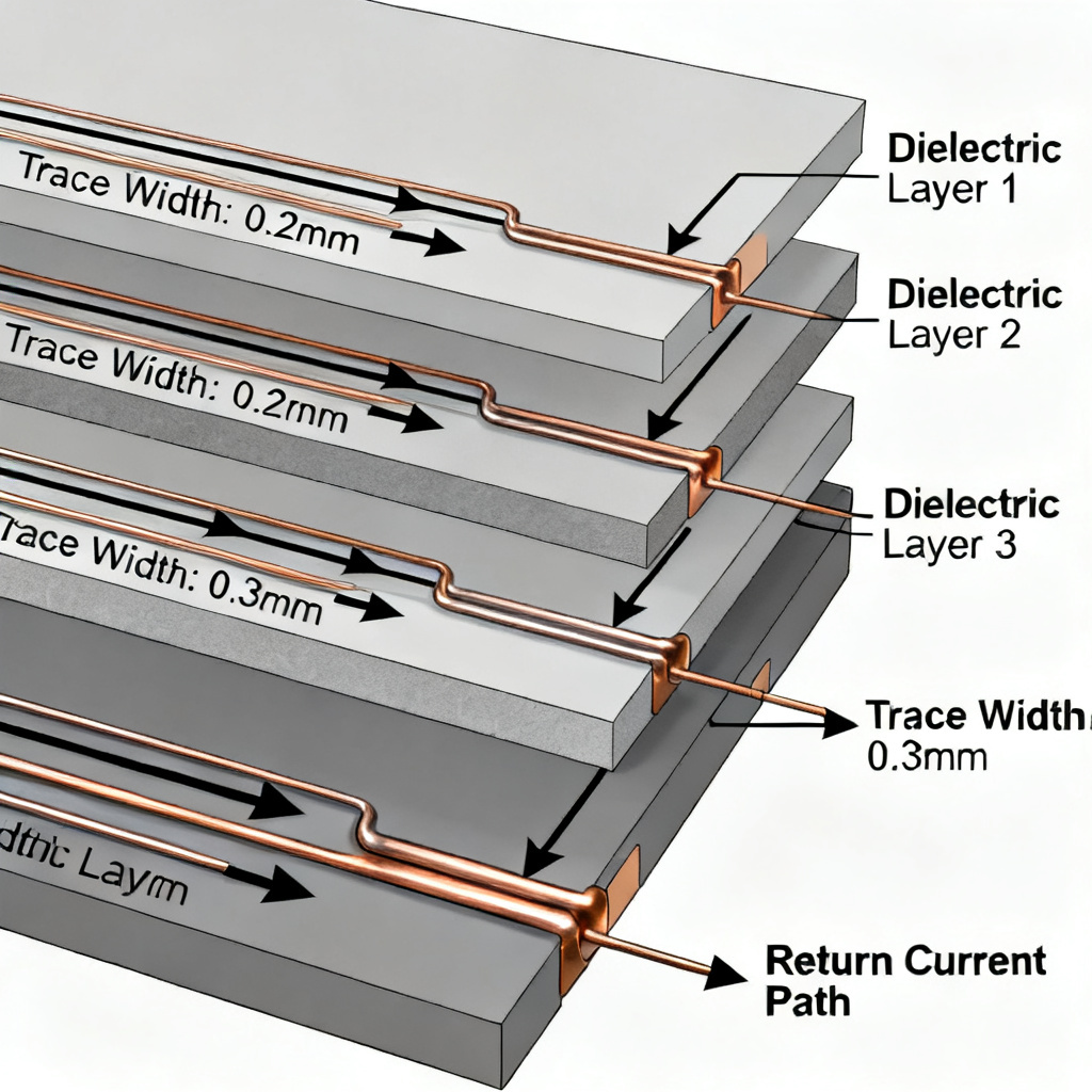
When board thickness affects crosstalk in high speed PCB, a thinner dielectric (e.g., 4 mils) tightens return current coupling, reducing loop area and mutual inductance. Conversely, a thicker dielectric (e.g., 10 mils) increases loop area, raising both self-inductance and mutual inductance. This fundamental relationship means crosstalk magnitude rises with increasing dielectric height.
Return Current Path and Signal Integrity
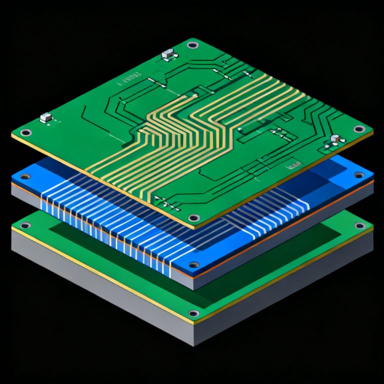
In microstrip and stripline configurations, board thickness affects crosstalk in high speed PCB by altering the distance between signal trace and reference plane. A thinner core reduces the loop area, lowering inductive crosstalk, but increases capacitance per unit length—a trade-off every designer must evaluate.
Unexpected Trade-Off #1: Thicker Board, Worse Crosstalk in High Speed PCB
One of the most counterintuitive findings is that increasing total board thickness—especially in stripline layers—can actually worsen crosstalk in high speed PCB, not improve it. This paradox arises from the need to widen traces to maintain 50Ω impedance when dielectric thickness increases.
The Stripline Paradox Explained
In a 4-layer board, if you increase the core thickness between signal layers, board thickness affects crosstalk in high speed PCB by forcing wider traces. Wider traces have larger surface area for capacitive coupling, and larger loop areas extend magnetic field lines further. Simulations from industry experts (e.g., Eric Bogatin) show that doubling dielectric thickness from 4 mils to 8 mils can increase crosstalk by 3–6 dB.
Practical rule: For high-speed signals on inner layers, use a thin core (4–5 mils). Do not increase board thickness for mechanical rigidity without considering the crosstalk penalty.
Unexpected Trade-Off #2: Thinner Board, Higher Loss and EMI in High Speed PCB
While a thinner board reduces crosstalk, board thickness affects crosstalk in high speed PCB differently when considering dielectric loss and EMI. Thinner dielectrics require narrower traces, increasing conductor loss due to skin effect. At 10GHz+, a 5-mil trace has significantly higher resistance than a 10-mil trace.
Dielectric Loss and Material Selection
Board thickness affects crosstalk in high speed PCB also through material Df. Thinner prepregs (e.g., 1080 or 1067) have higher resin content, which can increase dissipation factor. For designs above 10Gbps, consider low-loss materials like Megtron 6 or Rogers 4350B to compensate.
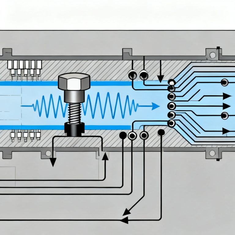
EMI and Via Stub Management
A thinner board means signal layers are closer to the board edge, increasing edge radiation and EMI susceptibility. However, board thickness affects crosstalk in high speed PCB via stub length: thicker boards have longer via stubs, creating resonant notches in insertion loss. Back-drilling becomes essential for thick boards above 10Gbps.
Unexpected Trade-Off #3: Dielectric Constant and Effective Crosstalk in High Speed PCB
Board thickness affects crosstalk in high speed PCB through effective dielectric constant (Dk_eff). Higher Dk materials (e.g., FR-4 at 4.5) increase capacitive coupling, worsening crosstalk. Lower Dk materials (e.g., Rogers at 3.0) reduce capacitance but may increase signal velocity.
Glass Weave Effect on Crosstalk
In standard FR-4, glass fibers (Dk ~6) and epoxy resin (Dk ~3) create non-uniform dielectric. When board thickness affects crosstalk in high speed PCB, the glass weave effect causes differential skew and mode conversion in differential pairs. Use thin prepregs with high resin content (e.g., 1067) for microstrip layers to minimize this effect.
How to Optimize Board Thickness for Crosstalk in High Speed PCB
Based on the three trade-offs above, here is a step-by-step guide to select optimal board thickness for crosstalk in high speed PCB:
Step 1: Define Signal Speed and Sensitivity
- Low speed (<1Gbps): Board thickness not critical. Use standard 1.6mm.
- Mid speed (1–10Gbps): Use thin core (4–5 mils) for signal layers. Total thickness 0.8–1.2mm.
- High speed (>10Gbps): Use hybrid stackup with thin cores (3–4 mils) for signals, thicker prepregs for power.
Step 2: Apply the Modified 3W Rule
When board thickness affects crosstalk in high speed PCB, use spacing ≥ 5 × H (dielectric height). For 5-mil dielectric, spacing should be at least 25 mils. For 10-mil dielectric, spacing must be 50 mils.
Step 3: Simulate with Field Solvers
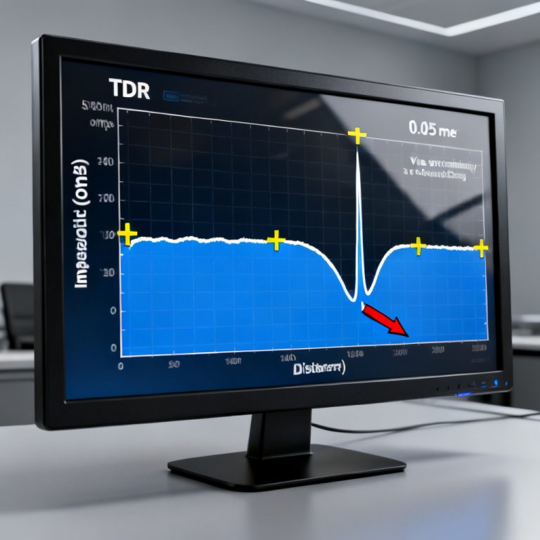
Use 2D field solvers (e.g., Polar Si9000, Ansys Q3D) to model NEXT and FEXT. Target crosstalk below -40 dB for NEXT and -50 dB for FEXT.
Step 4: Consider Differential Pairs
For differential signaling, use tightly coupled pairs with thin dielectric. Board thickness affects crosstalk in high speed PCB common-mode rejection—thin dielectrics improve CM-crosstalk performance.
Step 5: Optimize Power Plane Distance
Keep power and ground planes close (3–4 mils) to reduce PDN impedance and power integrity crosstalk.
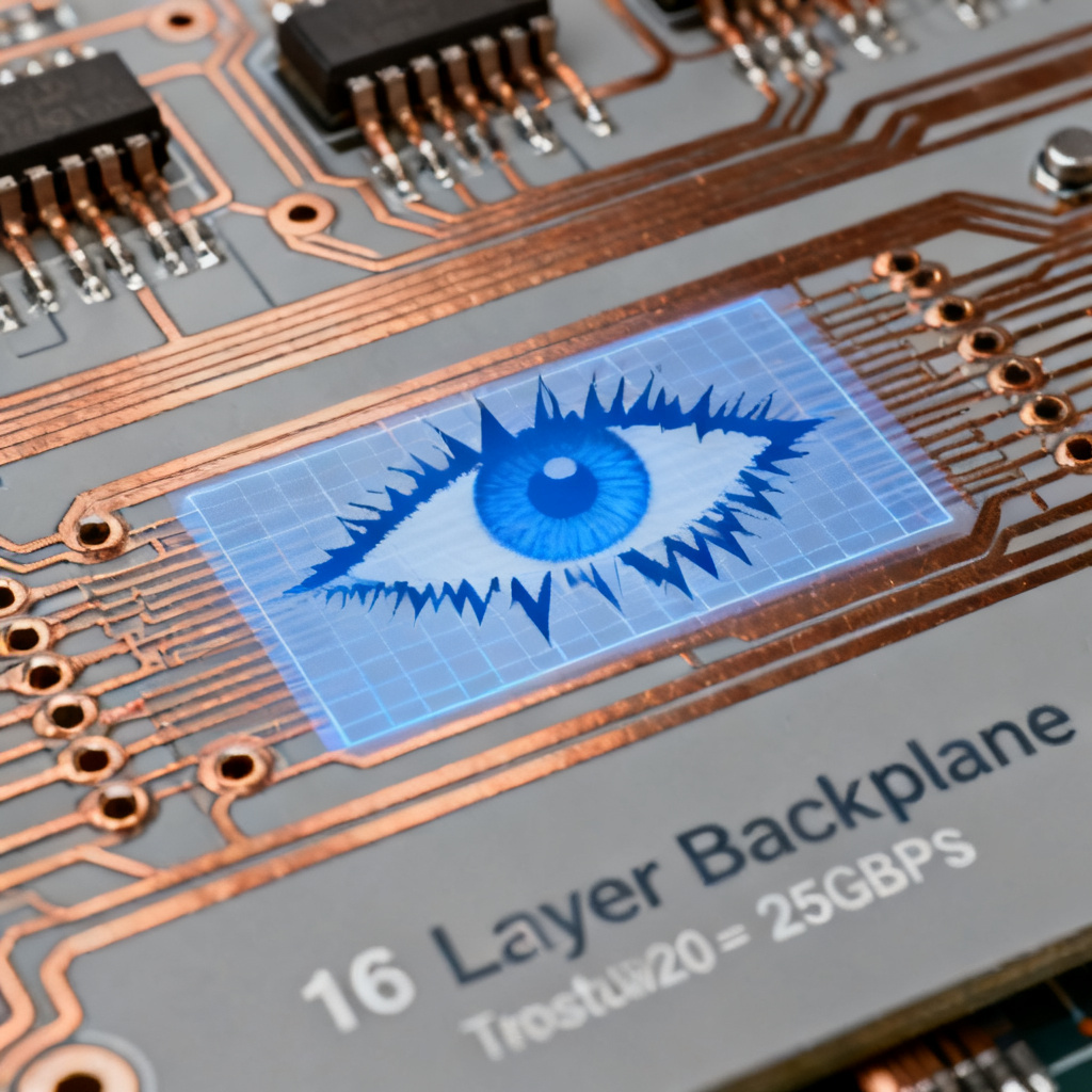
Case Study: 16-Layer Backplane at 25Gbps
| Parameter | Thick Board (2.0mm) | Thin Board (1.2mm) |
|---|---|---|
| Signal layer core thickness | 8 mils | 4 mils |
| Trace width for 50Ω | 10 mils | 5 mils |
| Trace spacing | 15 mils | 20 mils |
| Crosstalk at 12.5GHz | -35 dB | -48 dB |
| Eye height closure | 10% | 5% |
| Via stub requirement | Back-drilling needed | Shorter stubs |
Verdict: For 25Gbps+, thin boards win despite higher manufacturing complexity. Board thickness affects crosstalk in high speed PCB more than any other single parameter.
Summary of Key Trade-Offs for Board Thickness and Crosstalk in High Speed PCB
| Parameter | Thinner Board (0.8mm) | Thicker Board (1.6mm) |
|---|---|---|
| Crosstalk | Lower (tight return current) | Higher (larger loop area) |
| Dielectric loss | Higher (narrower traces) | Lower (wider traces) |
| EMI | Potentially worse | Better shielding |
| Via stub | Shorter, less resonance | Longer, needs back-drilling |
| Mechanical strength | Weaker | Stronger |
| Manufacturing cost | Lower (fewer layers) | Higher (more material) |
FAQ: Board Thickness and Crosstalk in High Speed PCB
How does board thickness affect crosstalk in high speed PCB?
Board thickness affects crosstalk in high speed PCB by changing the return current loop area. Thinner dielectrics reduce loop area, lowering inductive crosstalk, while thicker dielectrics increase loop area, raising crosstalk magnitude.
What is the optimal board thickness for crosstalk in high speed PCB?
For signals above 10Gbps, use thin cores (3–5 mils) for signal layers. Total board thickness can be 0.8–1.2mm for 4–6 layer boards. For thicker boards, back-drilling is essential to manage via stub resonances.
Does a thicker board always reduce crosstalk in high speed PCB?
No. Board thickness affects crosstalk in high speed PCB in a non-linear way. Thicker boards often worsen crosstalk due to wider trace requirements and larger loop areas, despite better EMI shielding.
What materials minimize crosstalk in high speed PCB?
Low-Dk materials (e.g., Rogers 4350B, Megtron 6) reduce capacitive coupling. Thin prepregs with high resin content (e.g., 1067) minimize glass weave effects. Board thickness affects crosstalk in high speed PCB most when using standard FR-4.