In high-speed PCB design, impedance mismatch is the root cause of reflection in transmission line systems, degrading signal integrity. When a signal encounters a change in characteristic impedance, part of its energy reflects back, causing overshoot, undershoot, and logic errors. This article explores the physics, mathematics, and practical solutions to eliminate reflections.
The Physics of Reflection: Why Impedance Mismatch Matters

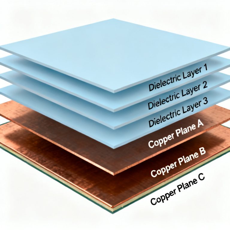
What is Characteristic Impedance?
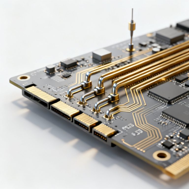
Characteristic impedance (Z₀) is the inherent property of a transmission line that determines the ratio of voltage to current for a traveling wave. In a PCB, this is determined by trace geometry (width, height above ground plane, dielectric constant, copper thickness). For microstrip or stripline, Z₀ is typically designed to be 50Ω or 100Ω differential for high-speed signals. When the signal propagates along a uniform trace with constant Z₀, it sees a consistent impedance. The signal energy is fully absorbed by the load if the load impedance (ZL) equals Z₀. However, any deviation—a change in trace width, a via, a connector, or a stub—creates an impedance discontinuity.
The Reflection Mechanism: The Instant of Impact
When a voltage wave (Vᵢ) traveling on a transmission line encounters an impedance discontinuity at point X, the line cannot instantly change its voltage and current. To satisfy Kirchhoff’s laws and boundary conditions, a reflected wave (Vᵣ) is generated traveling back toward the source. The amplitude and polarity of this reflected wave depend on the reflection coefficient (Γ), defined at the point of mismatch. The key insight from transmission line theory is that the reflected wave superimposes on the incident wave. If the mismatch is severe, the reflected wave can be nearly as large as the original signal, causing destructive interference.
The Mathematics of Reflection: Calculating the Reflection Coefficient
The Reflection Coefficient Formula
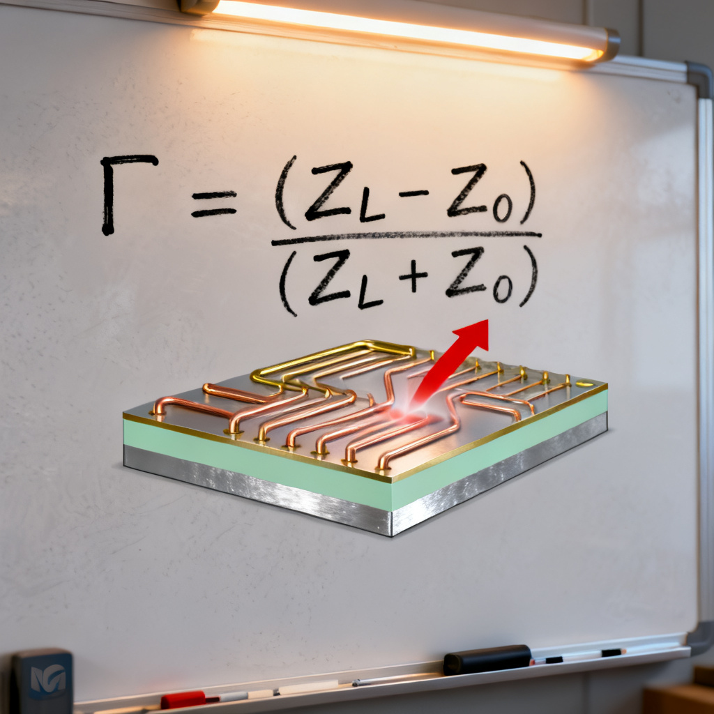
The reflection coefficient (Γ) at a discontinuity is given by: Γ = (Z_L – Z₀) / (Z_L + Z₀). Where Z_L is load impedance (or impedance seen at the discontinuity), and Z₀ is characteristic impedance of the transmission line. This equation tells us: perfect match (Z_L = Z₀) gives Γ = 0 (no reflection); open circuit (Z_L = ∞) gives Γ = +1 (full positive reflection, voltage doubles at open end); short circuit (Z_L = 0) gives Γ = -1 (full negative reflection, voltage goes to zero at short); mismatch (Z_L ≠ Z₀) gives Γ as a complex or real number indicating partial reflection.
The Voltage at the Discontinuity
The total voltage at the point of discontinuity is the sum of the incident and reflected waves: V_total = V_incident + V_reflected = V_incident × (1 + Γ). This explains why overshoot occurs: if Γ is positive (e.g., an open stub), V_total can exceed the driver’s output voltage. If Γ is negative (e.g., a low-impedance load), undershoot occurs. This superposition is the direct cause of signal degradation in high-speed digital systems.
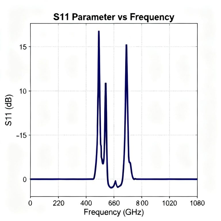
Time Domain Reflectometry (TDR) and Impedance Profile
A TDR instrument sends a fast step pulse down a transmission line and measures the reflected voltage over time. By analyzing the amplitude and polarity of reflected signals, you can pinpoint the location and nature of impedance mismatches. A positive reflection indicates a higher impedance (e.g., an open trace or narrow neck-down), while a negative reflection indicates a lower impedance (e.g., a via or stub). TDR is the gold standard for validating PCB impedance control.
Common Sources of Impedance Mismatch in High-Speed PCBs
Geometric Discontinuities
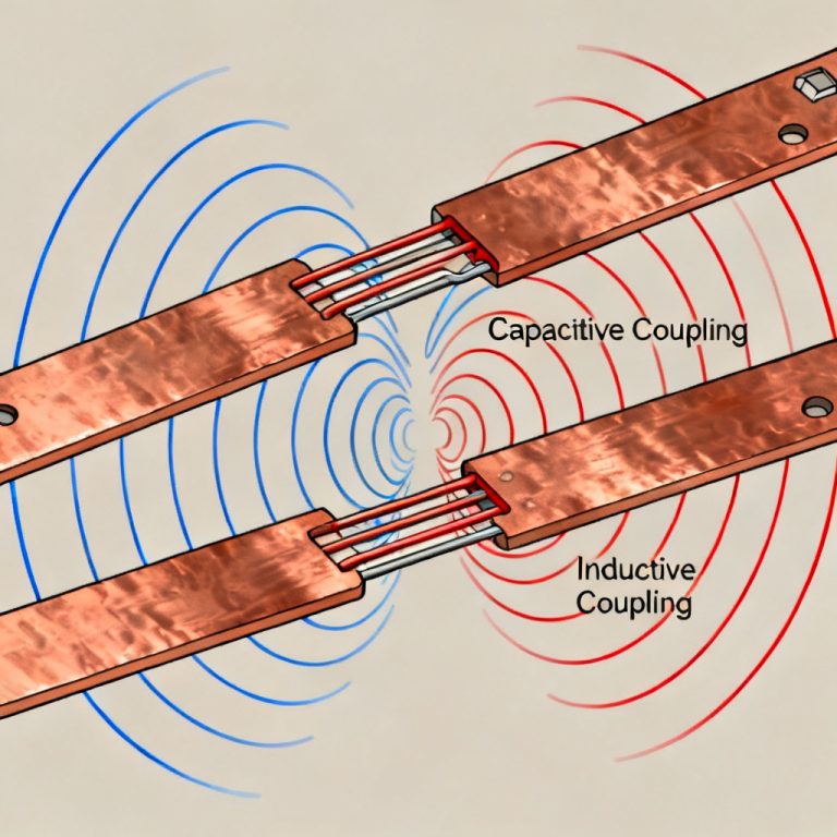
The most frequent cause of impedance mismatch is a change in trace geometry: trace width changes (a neck-down from 8 mils to 6 mils increases Z₀); trace bends (a 90-degree corner creates a capacitance discontinuity, lower impedance, mitigated with chamfered or curved corners); vias (a via barrel introduces an inductance discontinuity, higher impedance, and a capacitive pad, lower impedance, net effect usually a lower impedance dip); connectors (a connector’s impedance, often 50Ω, must match the PCB trace, otherwise the connector itself becomes a reflection source).
Stubs and Branch Lines
A stub is a short, unterminated branch off a main transmission line. At high frequencies, a stub acts like an open-circuit transmission line. When the signal reaches the stub junction, part of the energy goes into the stub, reflects off its open end, and returns to the main line, causing a delayed reflection. The severity depends on the stub length relative to the signal’s rise time. For digital signals, a stub longer than 1/10 of the signal’s rise-time distance can cause significant reflections.
Load Impedance Mismatch
Even if the trace impedance is perfect, the load (e.g., an IC input) may not match. Most high-speed inputs have high input impedance (capacitive), causing a mismatch. Series termination resistors (placed near the driver) or parallel termination (at the receiver) are used to match the load to Z₀.
Material and Manufacturing Variations
Dielectric constant (Dk) variations: FR4 has a Dk that varies with frequency and temperature, affecting Z₀. Copper thickness and etching tolerances: over-etching narrows traces, increasing Z₀. Dielectric thickness (prepreg) variations: a thicker dielectric layer reduces Z₀.
Practical PCB Design Rules to Eliminate Reflections
Controlled Impedance Design
The first step is to design your traces for a specific Z₀ (typically 50Ω single-ended or 100Ω differential). Use your PCB stack-up’s material properties and geometry to calculate the required trace width and spacing. Most PCB manufacturers offer impedance control services (e.g., ±10% tolerance). For high-speed designs, specify impedance control on critical nets (clocks, data buses, high-speed serial links).
Termination Techniques
Termination is the most effective way to absorb reflections at the load or source: series termination (source termination) places a resistor (R_s) near the driver such that R_s + R_driver = Z₀, matching the driver to the line, absorbing reflections from the load, common for point-to-point links; parallel termination (load termination) places a resistor (R_p) from the receiver input to ground (or to Vcc/2 for differential signals) equal to Z₀, absorbing the incident wave at the load, preventing reflection back to the source; AC termination uses a series RC network for capacitive loads; differential termination places a single resistor across the pair at the receiver equal to the differential impedance (e.g., 100Ω).
Stub Management
Keep stubs as short as possible: for high-speed signals, stubs should be less than 1/10 of the signal’s rise-time distance. For example, a 1 ns rise time signal has a rise-time distance of ~6 inches (in FR4), so a stub should be < 0.6 inches. Use daisy-chain routing: route signals from driver to receiver without branching. If multiple loads are required, use a bus topology with controlled impedance taps. Back-drilling: for multilayer PCBs, remove unused via stubs by back-drilling (drilling out the unused portion of the via barrel) to eliminate the stub’s reflection.
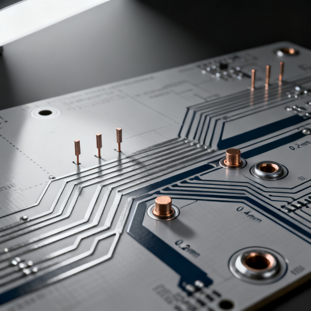
Via Optimization
Use ground vias near signal vias: place a ground via adjacent to a signal via to provide a return path and reduce the inductance discontinuity. Minimize via stub length: keep signal vias as short as possible by routing on layers close to the surface. Use microvias or blind/buried vias: these eliminate through-hole stubs entirely.
Simulation and Validation
Pre-layout simulation: use IBIS models to simulate reflections and determine optimal termination values. Post-layout simulation: extract S-parameters and run time-domain simulations to verify impedance profile. TDR measurement: after fabrication, use a TDR to measure the actual impedance profile of critical traces. Compare to your design targets.
Advanced Topics: Frequency-Dependent Reflections and Material Losses
Skin Effect and Dielectric Loss
At high frequencies (above 1 GHz), skin effect increases the resistance of the trace, and dielectric losses (tan δ) cause signal attenuation. These losses can alter the effective impedance seen by the signal, especially on long traces. While not a direct cause of reflection, they exacerbate the impact of mismatches by reducing the signal’s amplitude and increasing rise-time degradation.
Reflections in Differential Pairs
Differential signaling relies on two complementary signals. A mismatch in the pair’s common-mode impedance or a skew between the two signals can cause differential-to-common mode conversion, leading to reflections and EMI. To minimize this: keep the pair tightly coupled (controlled spacing); match the pair’s differential impedance to the driver/receiver; avoid asymmetrical routing (e.g., one trace longer than the other).
The Role of Return Path
A broken return path (e.g., a ground plane split under a high-speed trace) creates a large impedance discontinuity. The signal current must find an alternative path, causing a significant reflection. Always provide a continuous reference plane (ground or power) under high-speed traces.
Frequently Asked Questions (FAQ)
What is the root cause of reflection in transmission line?
The root cause of reflection in transmission line is impedance mismatch. When the characteristic impedance of the line does not match the load impedance, a portion of the signal energy is reflected back, causing signal degradation in high-speed PCB designs.
How does impedance mismatch affect signal integrity in high-speed PCBs?
Impedance mismatch causes reflections that lead to overshoot, undershoot, ringing, and logic errors. This degrades signal integrity in high-speed PCBs, especially in applications like PCIe 5.0, DDR interfaces, and high-speed serial links.
What are practical ways to prevent impedance mismatch in PCB design?
Practical ways include controlled impedance design (e.g., 50 Ohm characteristic impedance), proper termination techniques (series, parallel, AC), stub management, via optimization, and TDR validation. These methods eliminate reflections caused by impedance mismatch.
Comparison: Our High-Speed PCB Services vs. Standard Manufacturers
| Feature | Our High-Speed PCB Service | Standard Manufacturers |
|---|---|---|
| Impedance Tolerance | ±5% (tight control for impedance mismatch reduction) | ±10% (higher risk of reflection) |
| Stub Management | Back-drilling & microvia support | Limited stub removal |
| TDR Validation | In-house TDR for every critical net | Coupon testing only |
| Material Options | Low Dk/Df materials for high-frequency stability | Standard FR4 with higher loss |
| Design Support | Free impedance control PCB stackup review | Limited engineering assistance |
Glossary of Key Terms
- Impedance Mismatch: A condition where the characteristic impedance of a transmission line differs from the load impedance, causing signal reflection.
- Reflection Coefficient (Γ): A parameter that quantifies the amount of signal reflected at an impedance discontinuity.
- Characteristic Impedance (Z₀): The inherent impedance of a transmission line, typically 50Ω for single-ended or 100Ω for differential pairs.
- Time Domain Reflectometry (TDR): A measurement technique used to locate and characterize impedance mismatches in transmission lines.
- Signal Integrity: The quality of an electrical signal in terms of its shape, timing, and noise immunity, directly affected by impedance mismatch.
- Differential Pair: Two complementary traces used for high-speed signaling, requiring matched impedance to avoid mode conversion.