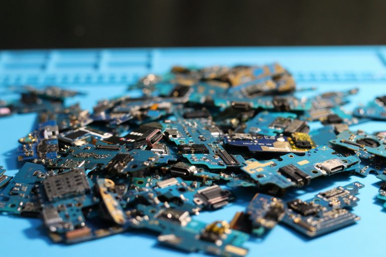
Modern compact electronic devices, high-frequency communication systems and high-density semiconductor packaging all require advanced multilayer PCB construction that standard single-cycle pressing cannot fulfill. Sequential lamination hdi pcb serves as the core manufacturing method to realize layer-by-layer build-up for reliable HDI structure and stable high-speed circuit performance. Understanding sequential lamination hdi pcb is essential for engineers working on high-density designs.
Different from conventional one-time lamination that bonds all layers in a single run, this process manufactures PCBs through multiple staged cycles. Between each pressing phase, manufacturers complete precision laser drilling, copper electroplating, via filling and circuit patterning. This layered production mode enables blind vias, buried vias and stacked microvias, helping design teams reduce board size, improve routing density and maintain stable impedance control. The PCB Manufacturing & Testing Guidelines provides a complete overview of all manufacturing processes, including sequential lamination hdi pcb. This guide integrates industry authoritative standards, real manufacturing experience and engineer-oriented DFM specifications.
Table of Contents
- 1. What Is Sequential Lamination? Core Definition & Engineering Purpose
- 2. Main Types of Sequential Lamination by Press Cycles
- 3. Complete Sequential Lamination Process Flow (1+N+1 HDI Standard Case)
- 4. Key Manufacturing Challenges & Industry Verified Solutions
- 5. Essential DFM Design Rules for Sequential Lamination PCB
- 6. Sequential Lamination vs Standard Traditional Lamination
- 7. Sequential Lamination Pre-Production Checklist
- 8. Industrial Applications of Advanced Lamination Technology
- 9. Key Takeaways
- 10. FAQ About HDI Sequential Lamination
- 11. Custom Project Evaluation & PCB Quotation Support
What Is Sequential Lamination? Core Definition & Engineering Purpose
Sequential lamination hdi pcb is an advanced multilayer PCB fabrication technique that constructs high-density circuit boards through multiple independent staged bonding cycles. Instead of combining all substrate and copper layers in one pressing operation, the board is built gradually in separate production stages. This is the foundation of sequential lamination hdi pcb manufacturing.
The core logic focuses on incremental layer construction. Fabricators first produce a complete inner core board, then attach build-up materials for partial lamination. After each pressing round, teams conduct laser microvia drilling, electroless copper plating, via filling and circuit imaging before starting the next lamination cycle. Every intermediate step strictly controls dimensional stability and layer alignment to guarantee long-term product reliability in sequential lamination hdi pcb production.
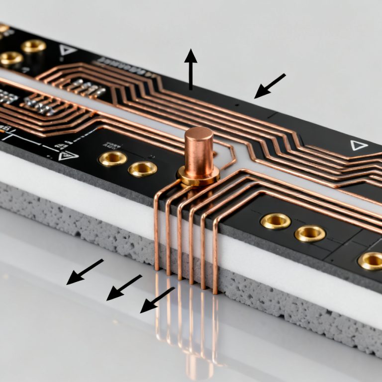
This manufacturing approach solves many bottlenecks in high-end hardware design. It naturally supports partial-layer interconnection structures that cannot be achieved by traditional through-hole design, effectively eliminating long via stubs that cause signal reflection and crosstalk in high-frequency scenarios. It also adapts to ultra-fine pitch BGA layout requirements, making device miniaturization and high-density routing fully achievable. For detailed HDI structure information, the HDI PCB Manufacturing Guide provides comprehensive coverage of stackup arrangements that rely on sequential lamination hdi pcb technology.
Core practical purposes of this advanced fabrication method:
- Realize precision blind vias and buried vias without damaging internal layer structure
- Support mainstream HDI stack structures including 1+N+1, 2+N+2 and any-layer design
- Optimize high-speed signal integrity by removing redundant through-hole stubs
- Sustain consistent dielectric performance for precise impedance control
- Reduce overall PCB footprint while maintaining mechanical strength and thermal stability
Main Types of Sequential Lamination by Press Cycles
Production complexity and structural capability in sequential lamination hdi pcb are directly determined by the number of lamination press cycles. More pressing stages bring higher routing density and more flexible interconnection design, while also raising manufacturing difficulty, extending production lead time and increasing overall cost.
| Lamination Cycles | HDI Structure | Complexity | Core Characteristics | Typical Application |
|---|---|---|---|---|
| 1 Time | Standard Multilayer | Basic | Only through-hole vias; no blind/buried via | Industrial control, low-density consumer |
| 2 Times | 1+N+1 HDI | Medium | One build-up layer each side; supports single blind vias | Wearable devices, IoT hardware, entry-level mobile |
| 3 Times | 2+N+2 HDI | High | Double build-up layers; allows stacked microvias | Automotive ADAS, 5G modules, high-end portable |
| 4+ Times | Any-Layer / ELIC | Extreme | Full interconnection between every layer | AI servers, aerospace, semiconductor packaging |
Design teams should always select the minimum press cycles that match project requirements for sequential lamination hdi pcb. Unnecessary over-design will only increase production cost and warpage risk without bringing actual performance improvement.
Complete Sequential Lamination Process Flow (1+N+1 HDI Standard Case)
The 1+N+1 structure with two lamination cycles is the most widely adopted and cost-effective solution in industrial production. Its workflow represents the standard manufacturing logic applicable to all multi-stage build-up boards in sequential lamination hdi pcb manufacturing.
Step 1: Inner Core Board Fabrication
Manufacturers start with high-Tg FR-4 or low-loss high-speed dielectric substrates. Inner layer circuit etching, conventional mechanical drilling and buried via electroplating are completed first. Thermal aging pretreatment is implemented in advance to release internal material stress and minimize expansion or deformation during repeated high-temperature processes in sequential lamination hdi pcb production.
Step 2: First Stage Lamination
RCC resin coated copper foil is attached evenly on both sides of the prepared inner core panel. Under precise temperature, pressure and time parameters, the first high-pressure lamination is completed to form preliminary upper and lower build-up layer structures for sequential lamination hdi pcb, ensuring tight resin flow and stable layer bonding.
Step 3: Laser Drilling for Blind Microvias
UV or CO₂ laser drilling technology is applied to fabricate tiny blind vias connecting outer layers with adjacent inner layers. The Laser Drilling Guide provides detailed information on microvia formation parameters that support sequential lamination hdi pcb manufacturing.
Step 4: Electroless Plating and Via Filling
Blind via inner walls are metallized through electroless copper deposition, followed by pulse electroplating and full copper via filling. Fully filled vias maintain flat board surface, support stacked via layout and effectively reduce signal attenuation in high-speed transmission circuits for sequential lamination hdi pcb designs.
Step 5: Second Overall Lamination
The semi-finished build-up panel is integrated with the inner core for secondary integral pressing. This step consolidates the overall stack structure, eliminates internal gaps and enhances the PCB’s mechanical strength and thermal cycle resistance.
Step 6: Outer Layer Circuit and Final Post-Processing
Proceed with outer layer pattern transfer, circuit etching, solder mask coating and surface treatment. Finished boards undergo strict quality inspection including AOI optical scanning, X-ray via detection, impedance testing and layer alignment verification before delivery.
Key Manufacturing Challenges & Industry Verified Solutions
Repeated thermal cycles and multiple pressing processes inevitably cause cumulative errors and material stability issues in sequential lamination hdi pcb. The following table summarizes the most common production obstacles, root causes and professional solutions.
| Challenge | Root Cause | Optimized Industry Solutions |
|---|---|---|
| Interlayer Alignment Deviation | Cumulative positioning error from repeated pressing | Optical automatic alignment system; high-precision vacuum pressing; unified substrate batch with pre-thermal aging |
| Microvia Surface Sink or Protrusion | Unstable electroplating current; inconsistent resin shrinkage | Optimize pulse plating parameters; high-fluidity filling resin; controlled slow cooling |
| Board Warpage & Dimensional Deformation | Multiple thermal histories; asymmetric stack layout | Low-CTE, high-Tg, anti-CAF stable materials; enforce symmetric stackup design |
| Elevated Production Cost | Extra procedures, precision equipment | Match lamination times strictly with design needs; optimize panel layout |
| Mass Production Yield Fluctuation | Manual operation deviation; unstable parameters | Standardize full-process SOP; AOI and X-ray full inspection; automated production lines |
Early design optimization and manufacturer process standardization can effectively reduce these risks and ensure stable yield for both prototype and mass production orders in sequential lamination hdi pcb projects.
Essential DFM Design Rules for Sequential Lamination PCB
PCB designers must follow dedicated DFM guidelines for multi-stage lamination projects. Proper design specifications help avoid manufacturing rework, layer misalignment, board warpage and unsatisfactory high-speed signal performance in sequential lamination hdi pcb.
Symmetric Stackup Requirement
Maintain strict symmetry in dielectric thickness, copper weight and layer distribution based on the central core. Asymmetric layout easily triggers severe warpage after multiple thermal pressing cycles in sequential lamination hdi pcb manufacturing.
Controlled Blind Via Depth
For 1st-order HDI structure, keep blind via depth within 4mil. Excessive depth leads to incomplete laser drilling and insufficient copper plating coverage.
Reserve Alignment Tolerance
Leave ±2mil stackup deviation margin in initial layout design to accommodate cumulative positioning errors from multi-cycle pressing.
Optimized Panel Layout & Fiducial Marks
Set standard board edge process strips and optical fiducial points properly. Reasonable panel arrangement improves material utilization and reduces batch dimensional deviation.
Unified High-Speed Material Selection
For high-frequency circuit designs, use consistent low-Dk/Df low-loss substrates. Avoid mixing different material models to ensure uniform thermal expansion coefficient and impedance stability.
Standard Microvia Pad Size
Reserve sufficient pad diameter for blind microvias to prevent ring cracks and open circuit risks caused by lamination pressure. Additional DFM guidelines for high-speed designs are available in the DFM Rules for High-Speed PCB guide, which complements sequential lamination hdi pcb design practices.
Sequential Lamination vs Standard Traditional Lamination
Understanding the core differences helps designers and buyers select the right process according to product performance and cost positioning for sequential lamination hdi pcb versus traditional methods.
| Comparison Item | Sequential Lamination | Standard One-Time Lamination |
|---|---|---|
| Blind & Buried Via Support | Fully supports all types | Only mechanical through-holes |
| Maximum Layer Capacity | Unlimited, any-layer compatible | Usually 20–24 layers |
| High-Speed Signal Performance | No via stubs, stable impedance | Long stubs cause reflection and crosstalk |
| Production Lead Time | Longer due to multiple cycles | Short, single pressing workflow |
| Manufacturing Cost | Higher | Lower |
| Applicable Scenarios | HDI miniaturized, high-speed, automotive, server, aerospace | Low-layer, low-density, cost-sensitive projects |
Sequential Lamination Pre-Production Checklist
- Confirm exact HDI structure type: 1+N+1, 2+N+2 or any-layer, and required lamination cycles
- Provide complete stackup drawing with dielectric thickness, copper weight and layer sequence
- Label position, aperture and depth parameters of all blind vias and buried vias
- Reserve interlayer alignment tolerance and thermal deformation margin per factory DFM standards
- Verify manufacturer’s maximum lamination capacity and mass production yield level
- Confirm compatibility of selected high-speed materials with multi-cycle thermal processes
- Optimize panel layout and fiducial position to match factory production specifications
Industrial Applications of Advanced Lamination Technology
Sequential lamination hdi pcb has become a necessary manufacturing solution for high-end industrial sectors. The technology is widely deployed across demanding applications:
- 5G Telecommunication: Base station and high-frequency modules requiring stable impedance and compact layout
- AI & Server Computing: High-layer any-layer HDI mainboards for dense chip packaging
- Automotive Electronics: ADAS intelligent driving boards and in-vehicle high-reliability control circuits
- Consumer Electronics: Ultra-thin smartphones, tablets and wearable miniature HDI PCBs
- Medical Devices: High-precision miniaturized circuit boards with long-term reliability requirements
- Aerospace & Industrial Control: High-layer, anti-vibration PCBs adapting to harsh working environments
Key Takeaways
- Sequential lamination hdi pcb is indispensable for modern HDI and high-speed PCB manufacturing, enabling blind buried vias, stacked microvias and any-layer interconnection
- Press cycles directly determine structural complexity, cost and lead time; choose minimum cycles that meet project requirements for optimal sequential lamination hdi pcb results
- Following symmetric stackup, blind via depth control and alignment tolerance reduces warpage and defects
- Most manufacturing challenges can be solved with high-stability substrates and experienced manufacturers
- Use the pre-production checklist before file release to improve design-manufacturing matching efficiency
FAQ About HDI Sequential Lamination
Q1: What makes sequential lamination different from standard PCB lamination for sequential lamination hdi pcb?
Standard lamination bonds all layers in one run; sequential lamination uses multi-stage pressing to realize blind and buried via structure for better signal integrity in sequential lamination hdi pcb.
Q2: What do 1+N+1 and 2+N+2 mean in sequential lamination hdi pcb design?
1+N+1 means one build-up layer on each side with inner core, requiring two lamination cycles. 2+N+2 has two build-up layers per side, needing three pressing cycles for stacked microvias in sequential lamination hdi pcb.
Q3: Do all high-speed PCBs need sequential lamination hdi pcb?
Not mandatory for all. It is highly recommended for fine-pitch BGA, dense interconnection and designs requiring via stub elimination for stable high-speed transmission using sequential lamination hdi pcb technology.
Q4: What is the recommended alignment tolerance for sequential lamination hdi pcb?
Reserve ±2mil tolerance in layout design to offset cumulative positioning errors from repeated pressing processes in sequential lamination hdi pcb manufacturing.
Q5: Does more lamination cycles equal better sequential lamination hdi pcb performance?
Not exactly. Excessive pressing increases cost, lead time and warpage risk. Select minimum cycles that satisfy your design requirements for optimal sequential lamination hdi pcb results.
Custom Project Evaluation & PCB Quotation Support
If you are developing HDI or high-speed PCB projects that require sequential lamination hdi pcb fabrication support, our professional engineering team can provide one-stop technical assistance tailored to your design.
We offer: Free HDI structure evaluation • Stackup manufacturability checking • DFM rule optimization • Blind via parameter consultation • High-speed material selection advice for your sequential lamination hdi pcb project
Share your Gerber files, stackup drawings and project requirements with our team today. We will deliver detailed DFM feedback, professional technical suggestions and a competitive quotation in the shortest time.
About HighSpeedPCBs.com
We are a specialized PCB design and manufacturing service provider serving industrial, automotive, medical, and communications OEMs worldwide. Our expertise in sequential lamination hdi pcb ensures your high-density and high-speed designs are manufacturable and reliable. Complete manufacturing process documentation is available in the PCB Manufacturing & Testing Guidelines.
© 2026 HighSpeedPCBs.com — Professional High-Speed PCB Solutions